 JasMoH
Guiding Design Goals and Philosophy for Lock in Amplifier:
Similar capabilities to the sr530. This is a common, workhorse instrument that I would love to have on my bench. The big features i’m going for are:
Expense: this should be “affordable”. I don’t have a hard number, but I want these to be maybe $30-$50 ea. in singles.
Extensibility and limitation of features: This is intended to be both a general purpose instrument, and a “first pass” design. This means I’m not going overboard with high expense or difficult LNA designs, crazy filter topologies, etc. for example, I haven’t selected a tuned JFET LNA, or the lmc6001 transimpedance amplifier for this reason. I’m also not adding a lot of microcontroller measurement or display systems. These can be reserved for either a version 2.0 design or external modules.
Specific key features:
nanoVolt sensitivity, single ended or differential.
femtoAmp sensitivity.
I’ll be happy if I get within an order of magnitude of these targets. It is acceptable to add an external preamplifier with a better noise figure if I really need it.
Selectable gain from nV to mV
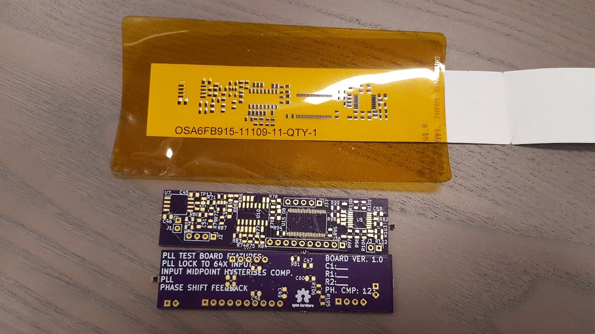
PLL:
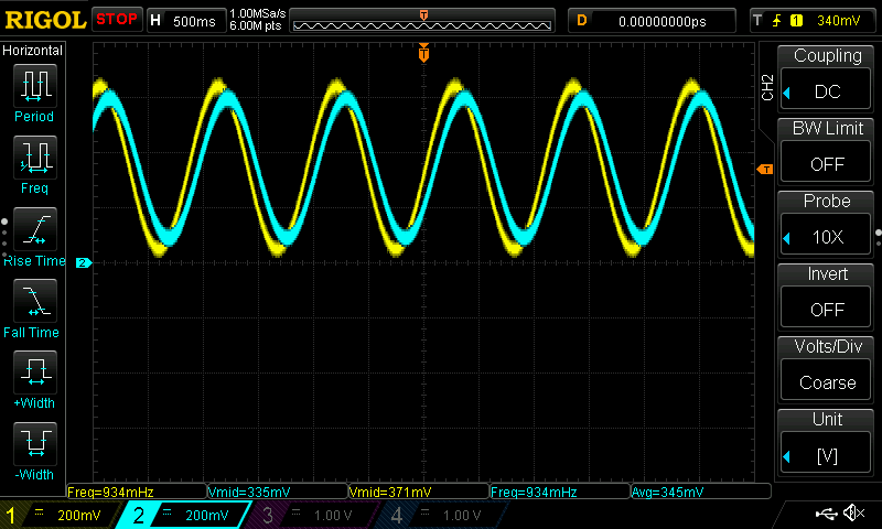
Modulation frequency selectable from 1 Hz to 100kHz. The ADA2200 requires a clock frequency 64X the modulation frequency, so that puts the PLL output at 64Hz to 6.4MHz. This is a weird frequency range to cover. I have not found any existing products that cover this use case that I’m happy with.
Input waveforms:
“Arbitrary” waveforms (within reason). The sr530 can lock to any input waveform that has sufficient pk-pk range and crosses it’s midpoint twice per cycle. This permits common logic schemes like TTL, as well as “real world” waveforms like a chopper wheel modulated photodiodes.
Since I’m ultimately looking to do photoacoustic spectroscopy, an optical chopper wheel is a very likely modulation scheme. This is a key feature that I want in an end system.
Filters:
Line filter
Adjustable bandpass filter around modulation frequency. I get this for free from the ADA2200, so I don’t intend to add dedicated filters, but this would be a good idea for a future version.


 Arno
Arno
 Clyne
Clyne
 Shrad
Shrad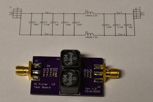
 Bharbour