 rob
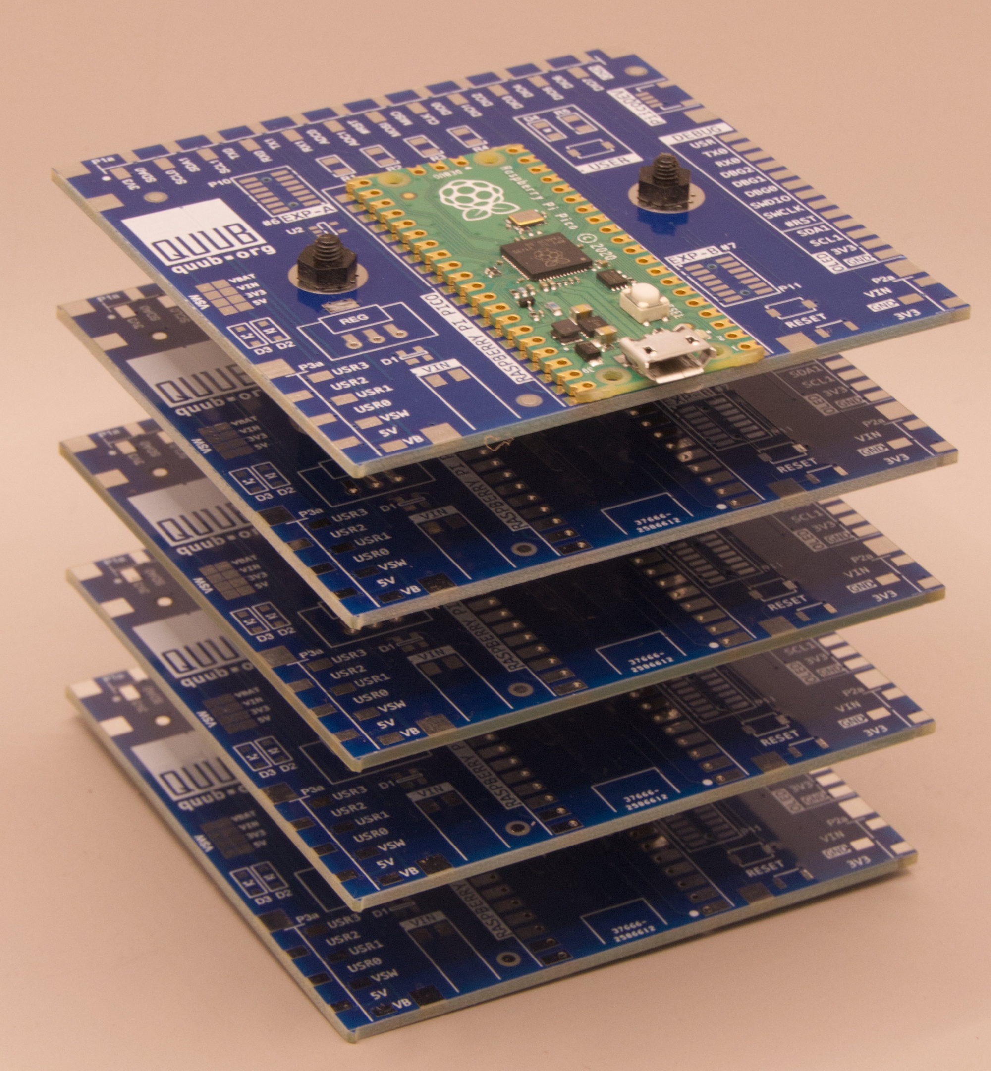
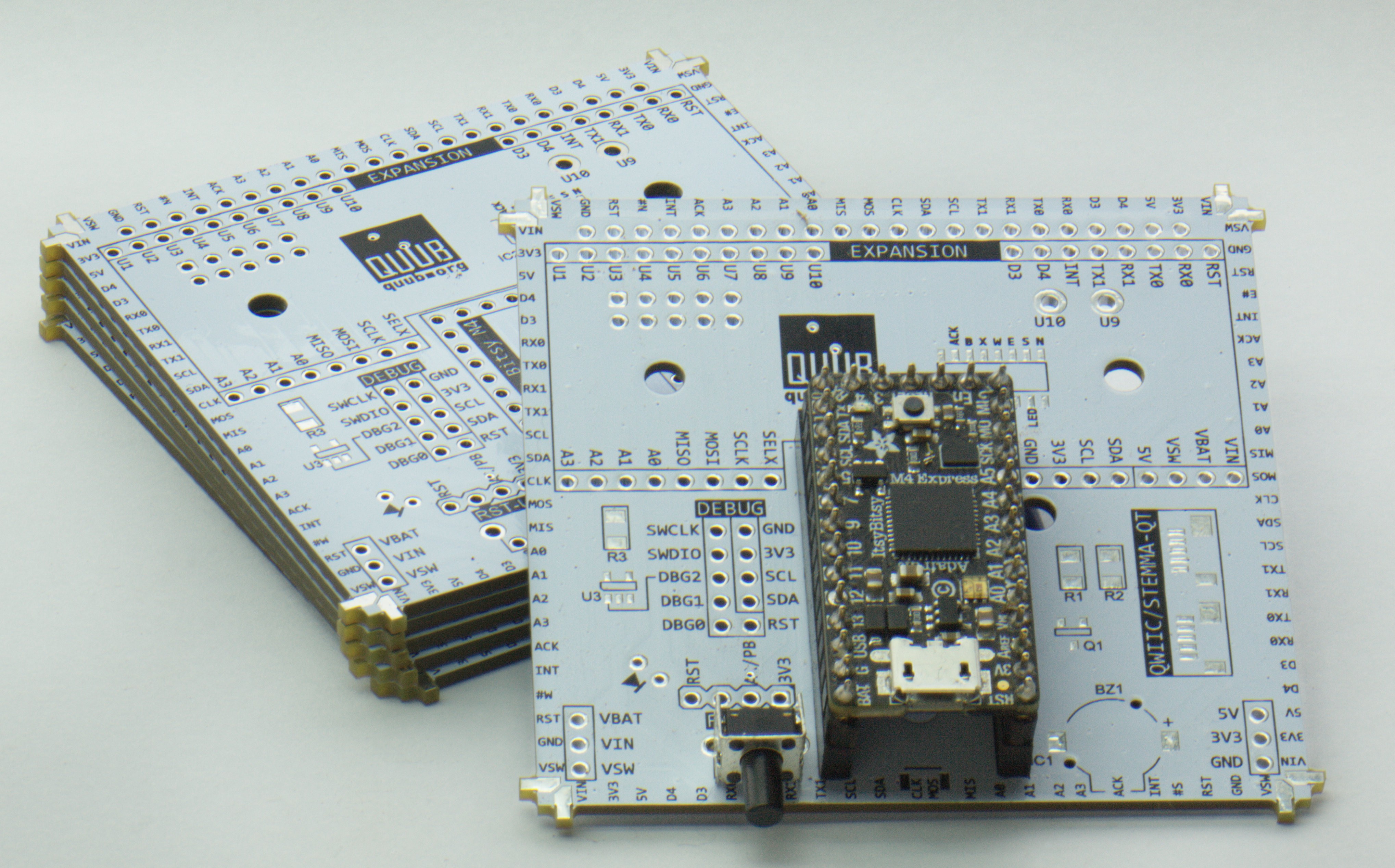
robQUUB is an open-source, micro controller system based on a core processor, addressable daughter boards which in turn can have addressable daughter boards, and remote IO modules. It is a general-purpose embedded microprocessor system, the form factor is based on a main MCU board and multiple stacked IO boards called "stackables" and smaller solder-on boards called "dockables".
This concept of up to 64 addressable boards makes for a very versatile system that can be configured for just about any imaginable application.
The target audience for the QUUB is more the serious hobbbyist and low-end BMAC (Building Monitoring and Control) applications, it's way overkill for a beginner's flashing-LED project, although can can be done as well.
The QUUB system has the following features.
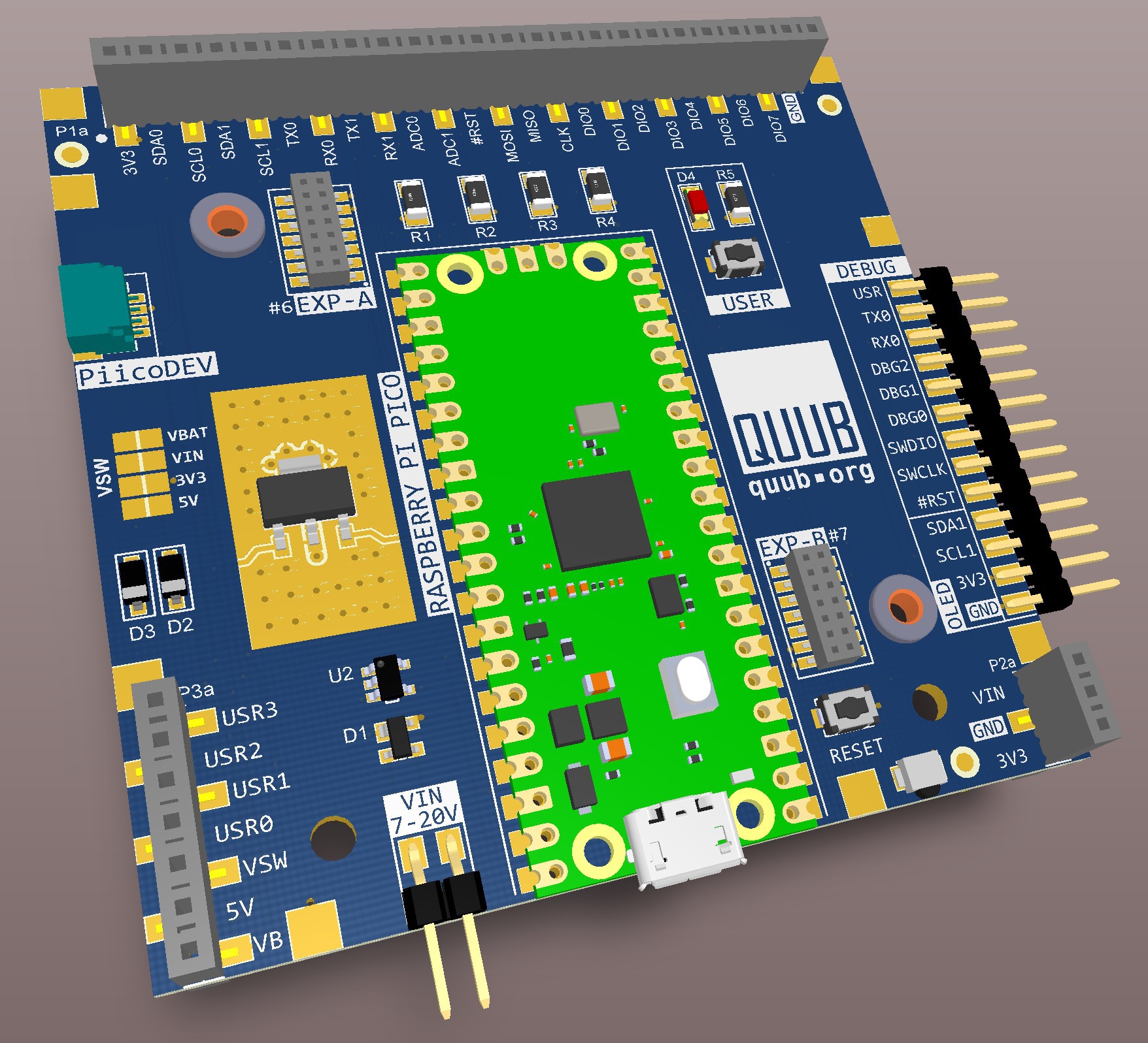
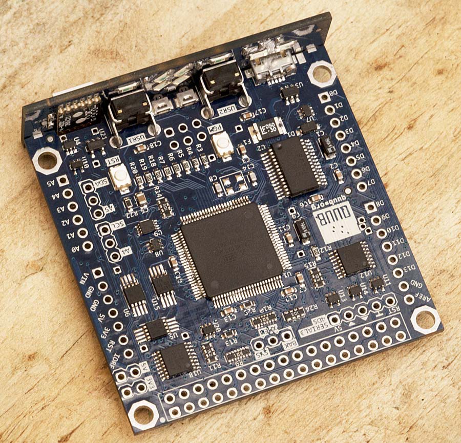
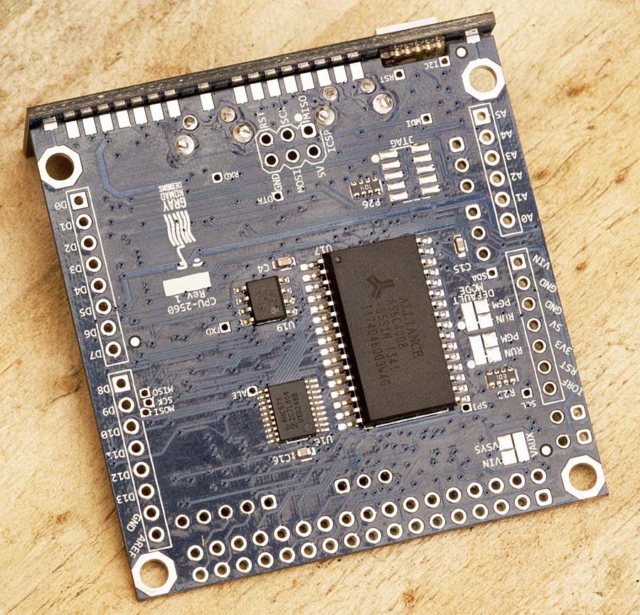
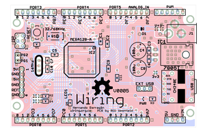
- The core processor board is an Raspberry Pi Pico module, this is a dual core 32-bit Cortex M0+ processor running at 133MHz.
- Medium size form factor, nominally 100 x 125mm (4 x 5 inches).
- A unique method of attaching front and rear panels.
- Up to 15 addressable daughter boards (stackables) can be stacked above or below the core processor.
- Up to 16 addressable devices on each stackable.
- Up to 4 addressable docking boards (dockables) on each Stackable.
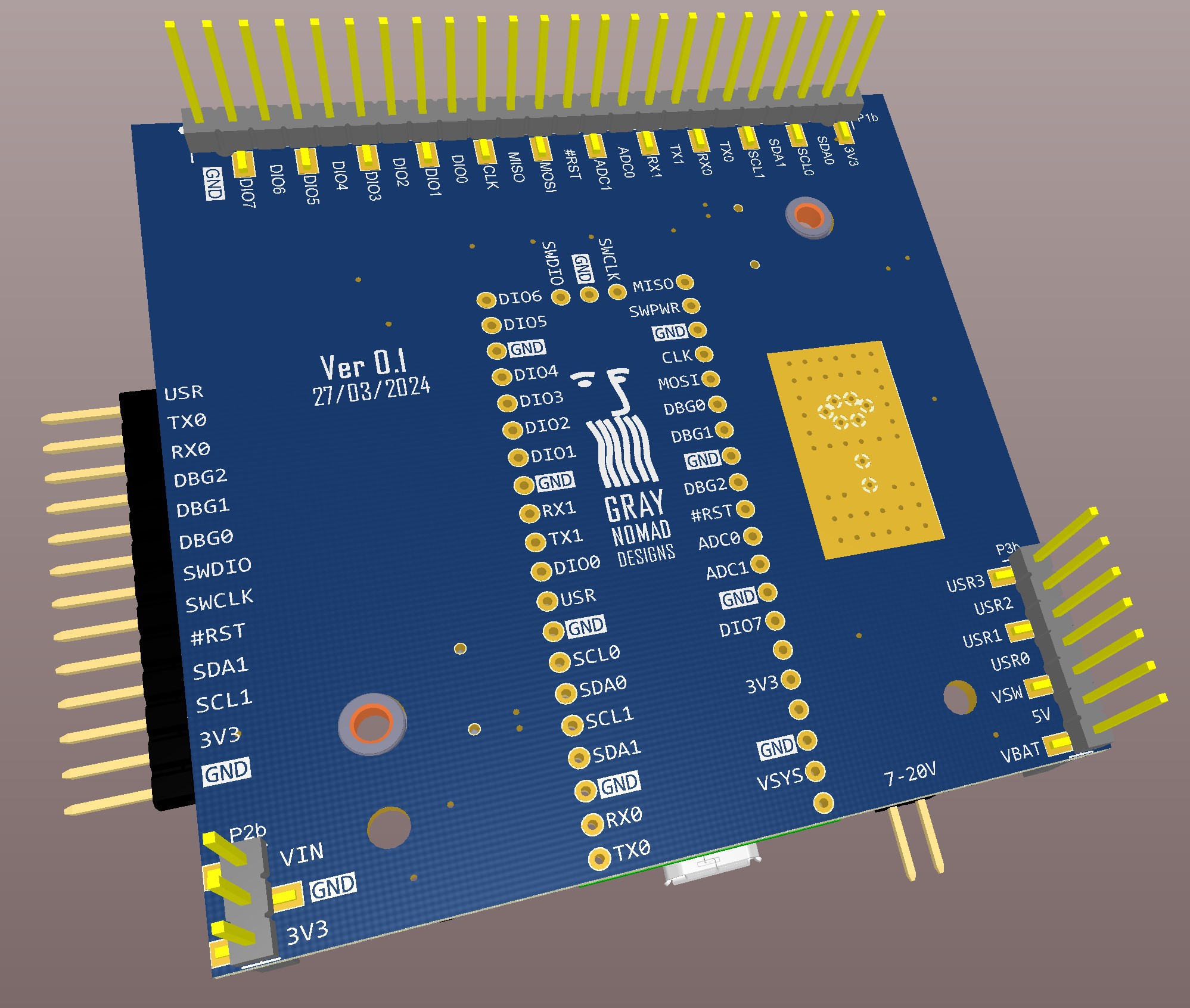
- Each dockable has access to UART, I2C, SPI, ADC, DIO, PWM, and various control signals.
- Allowance for dual dockables for functions than need more real estate.
- Each dockable can be shut down to conserve power.
- Each stackable and each dockable has a ID EEPROM that defines its IO capabilities for the MCU.
- Up to 256 vectored interrupts from these stackable modules
- Four docks on the MCU board for IO expansion, up to another 60 docks on a fully-loaded system.
- 36+3+3-way "stackplane" using stackable headers.
- The stackplane has provision for all power signals, I2C, SPI, 2x UART, 2x analogue in, up to 16 digital IO, four user-defined signals, and addressing of daughter boards.
- All 15 daughter boards can be addressed and can therefore share the same system IO lines.
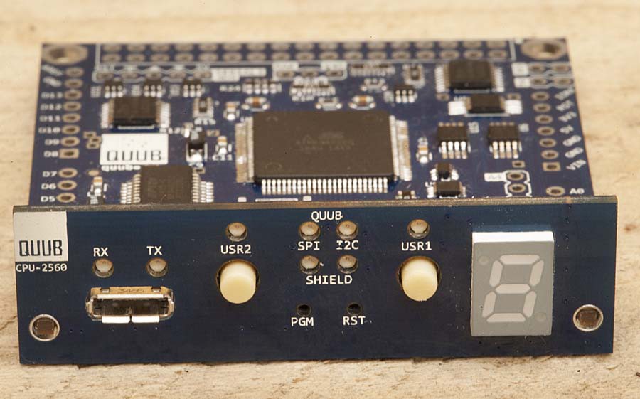
- Two front-panel accessible pushbuttons that are used for reset and a user input.
- One switched power signal that can be used by the MCU to shut down peripherals such as a GPS or wireless transmitter.
- Six mounting holes suitable for an M3 bolt or similar-sized screw.
- One-digit 7-segment LED display for a heartbeat or error code display.
- Provision for a .91" OLED display for debuging.
If you need a system with over 20 analogue inputs, or maybe 30 serial ports, or more than 200 digital IO connections, no problems, QUUB can do that and more.
Stackplane (backplane for the QUUB stack) The stackplane consists of three headers of 36, 3 and 3 connections. With the vast array of I2C and SPI peripheral IO chips now available it makes sense for larger and more complex applications to have a backplane with just a few signals that communicate with slave devices using one of these popular serial interfaces.
There are four user-defined signals on the stackplane, these signals pass up the entire stack and can be used by any stackable for whatever purposes. One example would be a power supply stackable sitting at the bottom of the stack that needs an ON/OFF switch and a power indicator LED at the top of the stack. Another might be to allow high-current devices to get power from a power-supply stackable via the stackplane.
Front and rear panels Provision is made to solder PCBs at right angles to the main PCB on the front and rear.The rear panel has access to all the stackplane signals, the front panel has the SPI, I2C, and power. These panels can be used to implement a user interface.
Bases A base is not normally required as the MCU board has no components on the solder side of the board. However the MCU may not be the lowest stackable and the one that is may have through-hole components. In this case a base board may be required to isolate the electronics from whatever the stack is mounted to.
Another reason to have a base board is to accommodate large components, for example a...
Read more »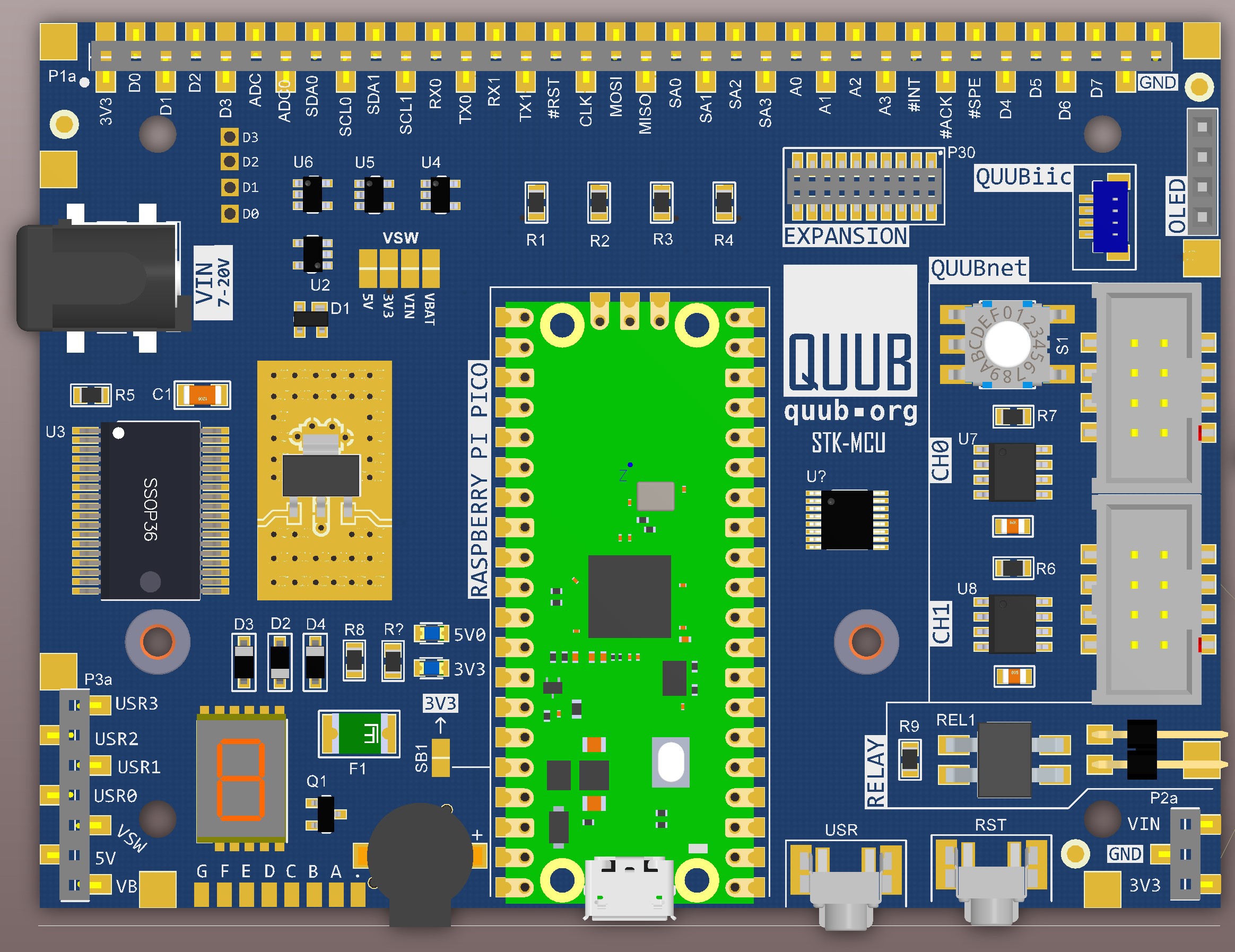
 The new CPU boards are here, I already have some changes in mind so I may not even test these one, we'll see.


 WestfW
 VASILIS VORRIAS
 Frank
Frank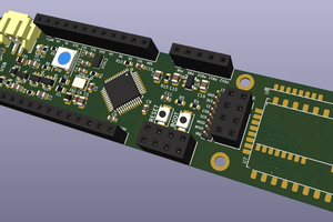
 Flavio