The Big One
-
Digital Control working
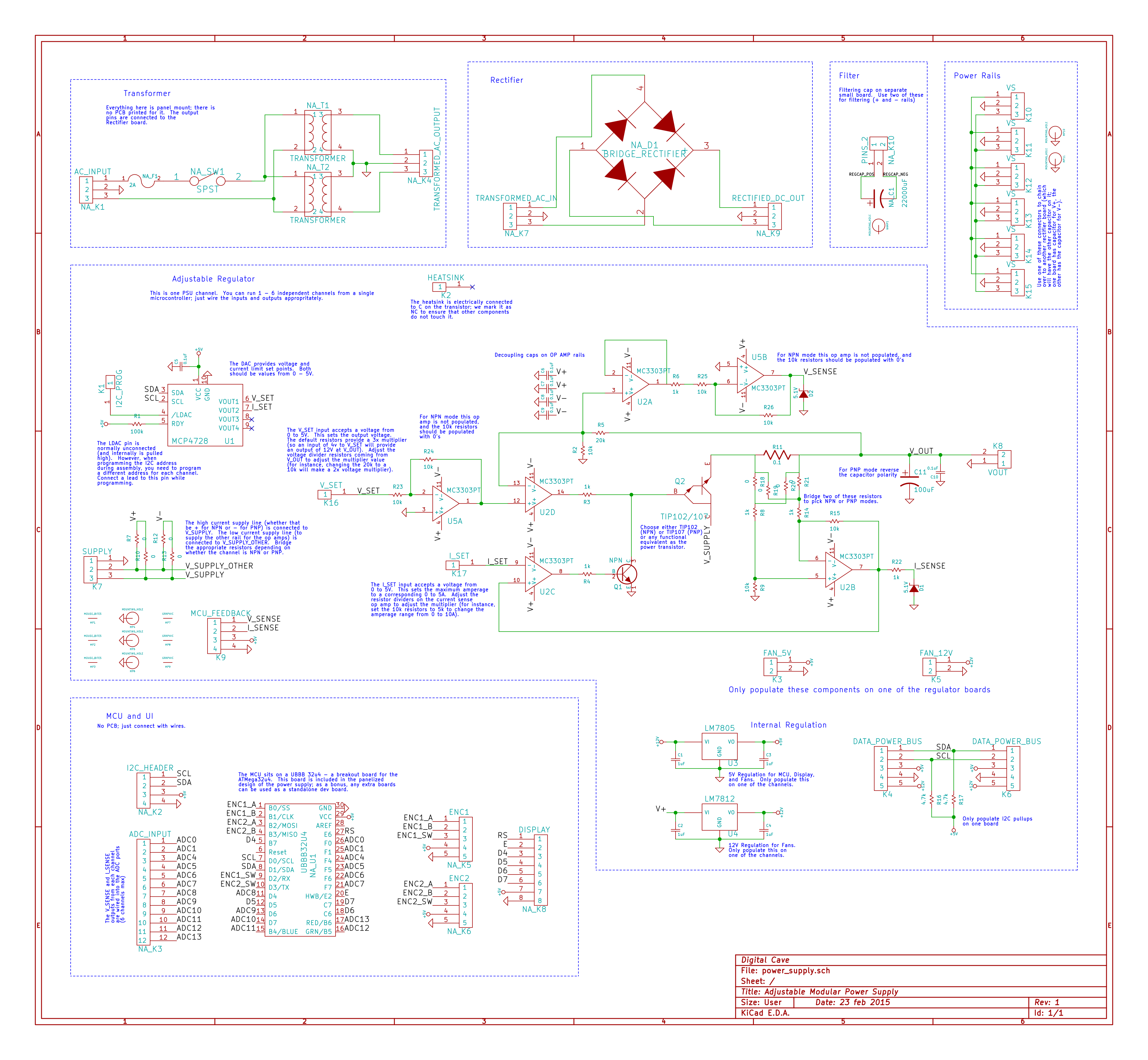
03/04/2015 at 22:39 • 0 commentsJust a brief comment... last night I got the digital control to work. This includes actual voltage / current readings (via ADC) as well as setpoints for voltage / current (via I2C DAC).
The only tricky bit was getting the I2C DAC wired up. I don't have any breakouts for MSSOP-10 packages, so I just dead bugged it using (very) thin wire on a bit of perfboard. It took a bit of fine-ironing skills, but it worked first try. A layer of hot glue for protection on top, and we are in business.
-
Breadboard Implementation (NPN)
03/02/2015 at 16:58 • 0 commentsI picked up the parts last week, and over the weekend I wired up a single channel (positive, using an NPN transistor) on the breadboard. Despite a couple false starts due to bad components (most notably the current limiting transistor, an old N2222 from my parts bin, caused all sorts of troubles before completely shorting out and exploding), it is now working. So far it only uses pots for V_SET and I_SET, the next step is to integrate the MCU.
I have done very little testing so far, but what I have seen looks promising. More info to come as it is available.
Along with the breadboarding comes some new design points:
- The interface for each channel is now purely analog (with values from 0 - 5V); the DACs are no longer on each channel. This allows for less wastage (all DAC channels are fully utilized), as well as giving an option for those people who don't want a dedicated controller board - simply use a potentiometer for VSET / ISET, and use your multimeter to read actual voltage / current outputs.
- Use a dedicated controller board with space for all DAC instead of re-using a 32u4 breakout board. This will make for easier wiring within the case (much fewer cables running all over the place).
- USB header is now on a separate board to allow for positioning in different arrangements within the case.
An updated schematic is below.
![]()
Cheers
-
New Design Details
02/23/2015 at 03:48 • 0 commentsThanks to everyone for all the helpful comments! Based on feedback from here and elsewhere, we have decided to move away from the power op amps, and go with a more traditional power transformer design.
The design allows for a positive output from 0 - 12V (using an NPN transistor) or a negative output from -12 - 0V (using a PNP transistor). There are a few differences in the circuit; when soldering up a positive channel vs. a negative channel you will bridge different 0-ohm resistors to configure how things work. Furthermore, there is a need for an additional op-amp IC to invert the control signal and the voltage sense output on the PNP version.
![]()
Simulations of both NPN and PNP versions are available at https://github.com/thebiguno/microcontroller-projects/tree/master/projects/power_supply/simulation (run these simulations in the very nice circuit simulator available at http://www.falstad.com/circuit/directions.html ).
This design was mostly made by myself and [Exot], taking inspiration from a number of online sources including Dave Jones' power supply design video and [Bogdan's] WIP power supply. The really neat thing (for me at least) is that I actually understand how it all works, which is much better than just using an off-the-shelf component like I was planning on previously.
The cost per channel is now much lower as well (a very rough estimate is $15 / channel, although that can easily be reduced if you scrounge some spare parts). The main microcontroller board, display, and encoders will run you about $20 if you source certain parts more intelligently (i.e. get the HD44780 display from eBay, not Digikey). The main power supplies can also vary in cost quite a bit... if you go with dual high amperage switch mode supplies (for positive and negative rails) it will run you about $60, but if you are only interested in positive (and if you don't care about having the voltage go all the way to 0), you should be able to run this off a wall wart.
I have decided that (eventually, at least) I will make 6 channels (4x positive, and 2x negative). I am going to power them with two switch mode power supplies connected together in series, with the connected rail tied to ground, giving me a +/- 15V supply (buying two switch mode supplies is still quite a bit cheaper than buying a high amperage transformer + the associated support components). [Exot] will have a smaller channel count, and will probably power his with a more traditional transformer + rectifier circuit, as he already has those on hand.
The board can be controlled via a microcontroller + I2C DAC (one DAC chip per channel), or can be controlled with a couple potentiometers. Basically the only requirement is that a varying voltage from 0-5V is applied to both the V_SET and I_SET inputs. Given the resistor values on the board, this will result in an output voltage of 3x the set point voltage (i.e. to get 12V out, apply a voltage of 4V to V_SET) and 1x the set point current (i.e. to get 3A max current out, apply a voltage of 3V to I_SET). You can easily adjust the value of the resistors to change these multipliers if you want more or less voltage / current output.
I plan on ordering the parts this coming week and putting them together on a breadboard, so that I can verify the operation in real life. I have already breadboarded this circuit using low power transistors, which is all I have available in my parts bin, and it works beautifully.
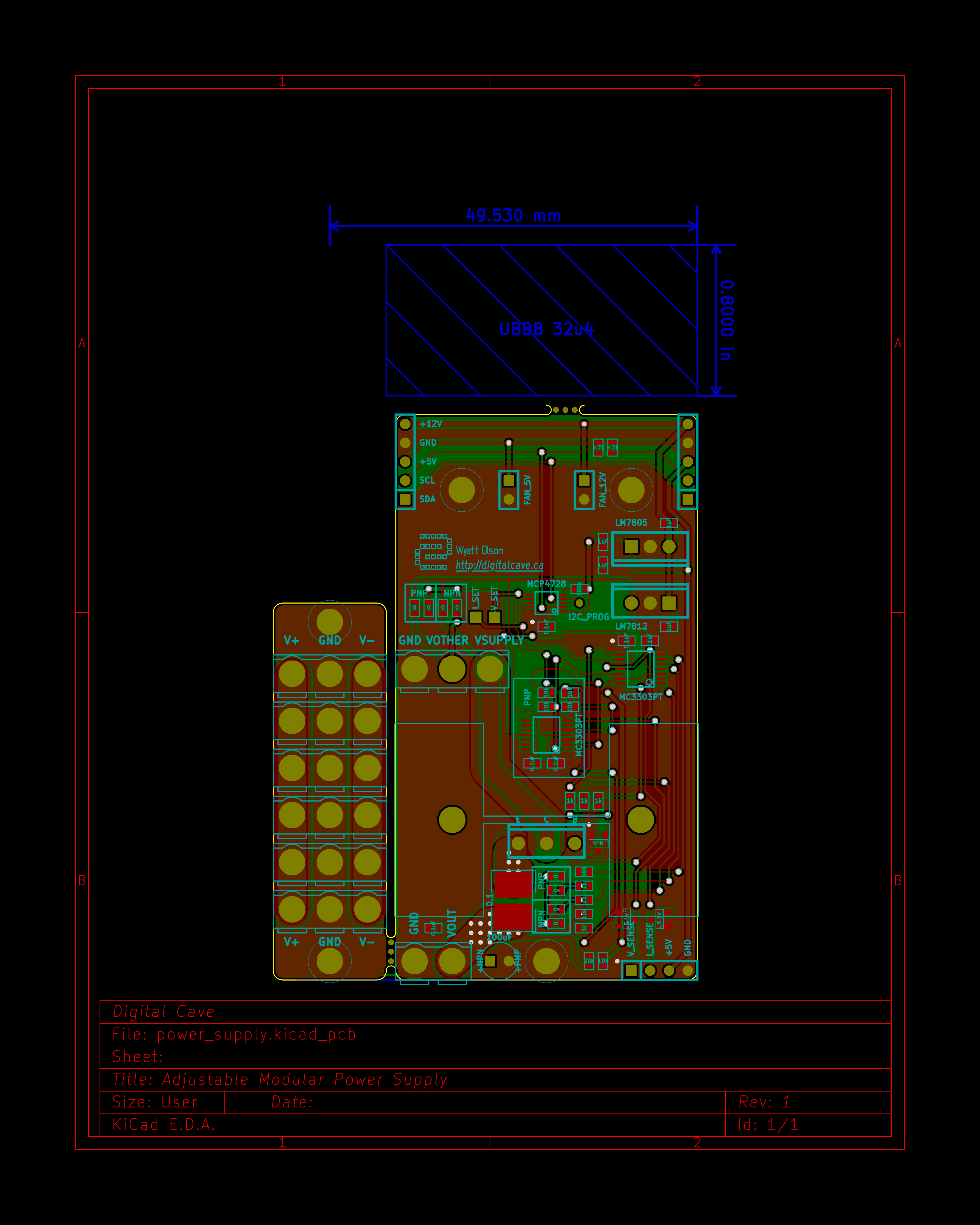
The boards are routed and ready to be ordered once the breadboard circuit is verified. The current version is below (the microcontroller will be in the blue shaded area, and I am not sure whether or not I will include a rectifier board):
I have a demo of the control software working, showing how the different modes will work and how to adjust values. Since this video was taken, I have received a 20x4 character display which I will be using instead of this smaller one:![]()
I think that just about covers it... even with all this work, I have yet actually make anything physical yet (well, other than the software demo and a low power breadboard version). Hopefully that will have changed by next weekend.
Cheers
-
Hackaday Comments
02/14/2015 at 22:53 • 0 commentsThanks to all those who submitted comments on the HaD article highlighting this project. [exot] and I are going over all that has been said, and will be making some modifications to the design to address the issues which have been brought up. This will doubtless take a couple of weeks at least. Stay tuned for further updates as the design solidifies.
Cheers
-
Alternatives to a Transformer
02/12/2015 at 16:29 • 0 commentsGiven the modular nature of this project, there is no requirement to use a transformer; all that is needed is a stable +/- voltage somewhere in the range of +/- 8-24V (depending on your output requirements). A transformer is the obvious simple way to do this, but there are others.
The simplest (most ghetto) way is to use two wall warts. This will give you the dual voltages needed, although it is probably a bit limited in current, depending on what wall warts you have on hand. The biggest downside is that it is ugly and clunky.
I am looking into something like this. In theory I can use two of them in the same configuration as the wall warts, and get a split rail. I am not sure on the details of this, though; if anyone has any experience doing this or has a link to somewhere that tells the specifics of what needs to be done, I would be very grateful.
Any other suggestions on the best way to get a +/- split rail supply on the cheap would be very much appreciated.
Cheers
-
(Potential) Change in Design Goals
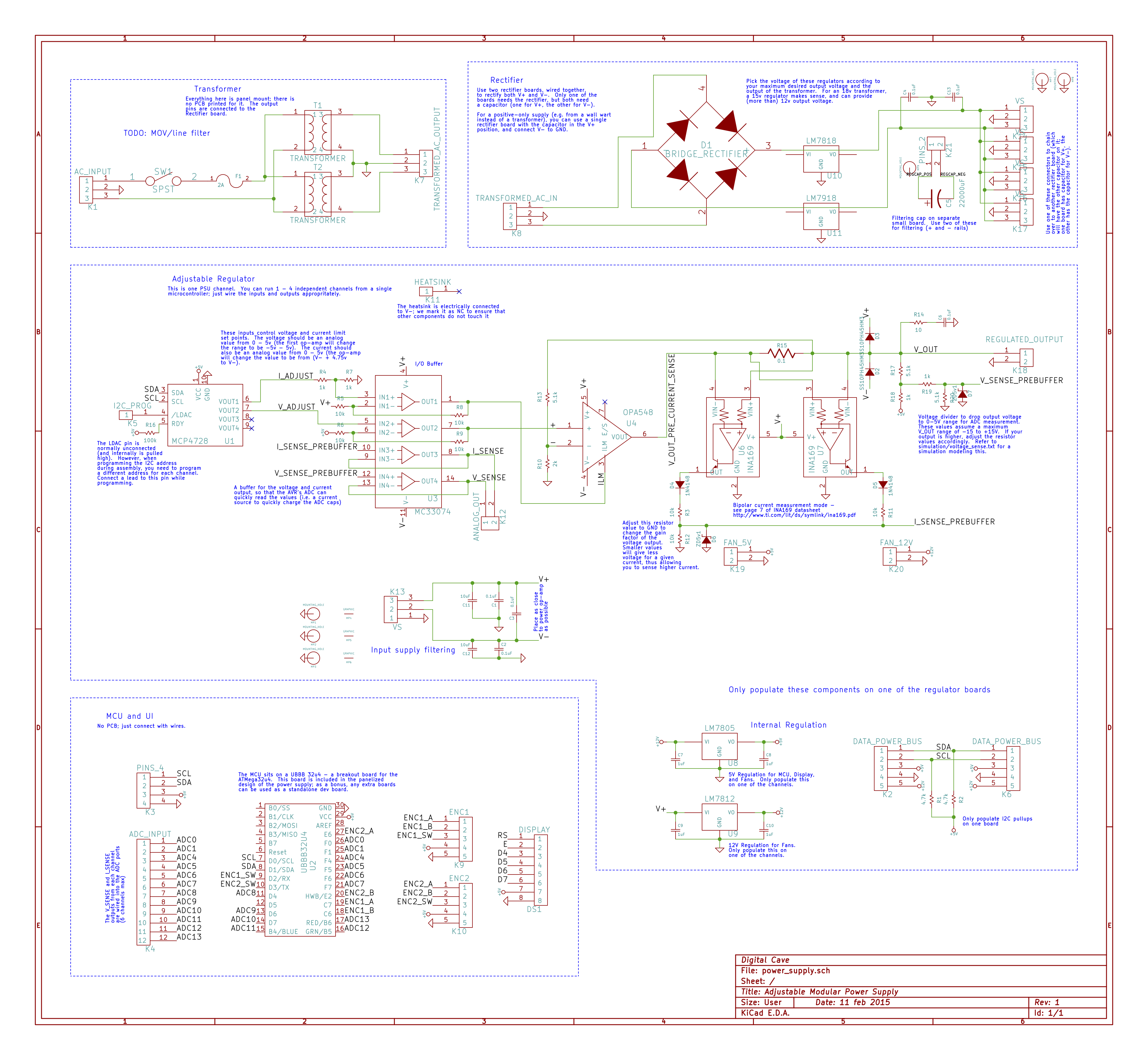
02/11/2015 at 20:39 • 0 commentsI have made a number of incremental changes to the design, and things are starting to be ready to start thinking of ordering a rev 1 board. However for this revision, I have removed support for picking one of either OPA549 or 548. The two chips have different pinouts, and adding components for both on the board (with the intent of only populating one) used a lot of space, plus limited how close I could place some components (such as bybass capacitors, which were supposed to be as close to the chip as possible).
I have thus removed the 549 package. In future revisions I may re-add it (possibly on it's own board so that I don't need to make compromises in the design.
As an overall status update, I am more or less happy with how things are looking now. I am going to be discussing the overall design with a friend who is also making one; if things look good there, I will be placing an order for components. The next step would be to prototype the thing on a breadboard (only low current output, of course), and, finally to order the boards. As timelines go, I hope to have the board order placed by the end of the month, and so will hopefully be doing the component order within a week. (Here's to the ability to stick to non-binding schedules!)
An updated schematic is below.
Cheers
![]()
-
Finalizing Requirements and First Draft Design
02/05/2015 at 01:20 • 0 commentsI have just updated the details section to update some of the changes made recently:
- Change from a "one-MCU per channel" design to a "single MCU controlling each channel" design - this will simplify firmware uploading (you can upload firmware over USB, and you only need to update it once rather than N times for N channels).
- Change from an XMega to an ATMega32u4 - this will simplify programming (more people have access to ISP programming gear vs. PDI) and development (since I already know the ATMega family inside and out).
- Adding the idea of programmatic control over USB (set voltage / current setpoints for each channel) as well as logging actual voltage / current readings. This will be done over Raw HID for driverless operation on all platforms.
- Removing the adjustable A/C output requirement. Trying to drive an A/C waveform at reasonable resolution (at least 256 samples) and frequency (at least 60Hz) over I2C is going to be too slow and processor intensive. Due to the MCU change, using a built-in DAC driven by DMA is no longer an option. However, all is not lost - I am still planning on bringing out the raw A/C output from the transformer, which means that I will have 18VAC at a high amperage available if needed.
- It makes extensive use of screw terminals for interconnecting the various boards
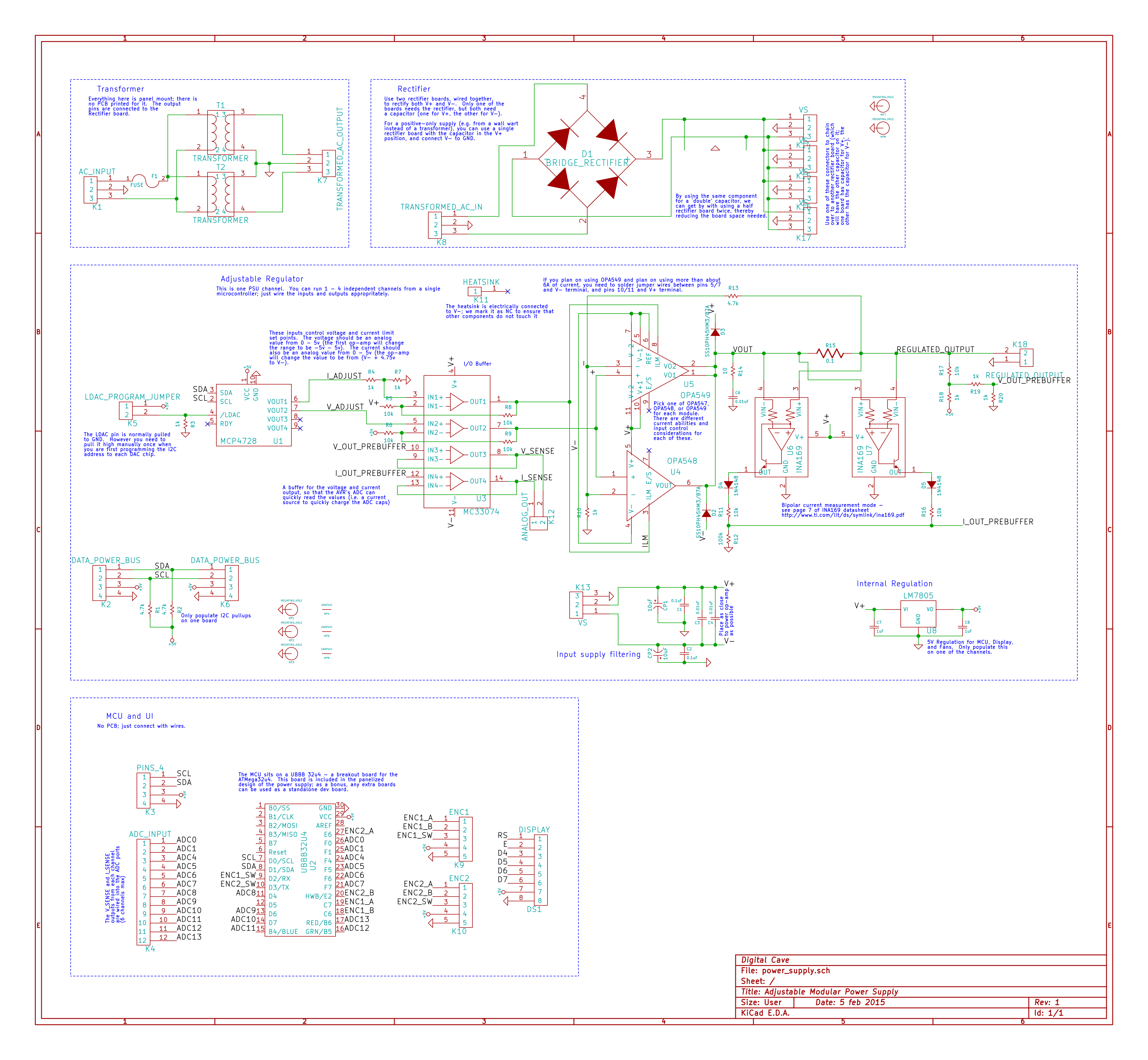
- When routing, I am targeting 1oz copper PCBs, which means the traces need to be thicker than usual. All traces are sufficient for a max of 8A / channel with the entire system limited by the transformer (to a reasonable point, of course), EXCEPT for the traces connecting the OPA549 to the V+ / V- inputs. For this section, if you plan on using more than about 6.5A you will need to solder on some thick jumper wires to carry more current.
In addition, I have the first draft of the schematic completed, along with a routed board coming in at just under 5x10cm (sans the UBBB32u4 controller board, which will be panelized in later). See both below:
![]()
![]()
-
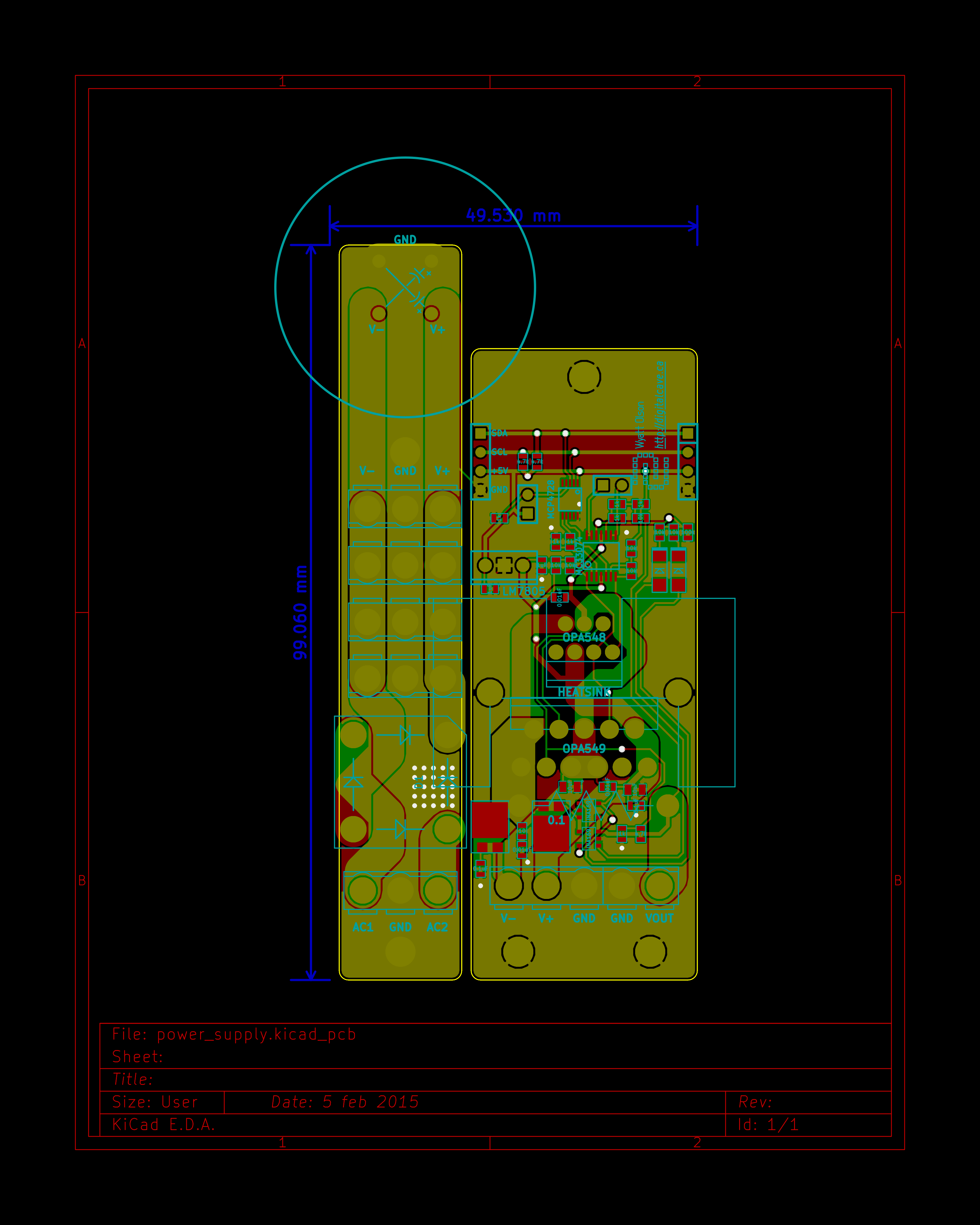
Board Size Update
02/04/2015 at 03:04 • 2 commentsWell, try as I might, I can't fit the thing into a 5x5cm board: there are just too many large components which need thick traces. Part of the problem is that I am trying to overspec the design; for instance, I am supporting both the 3A OPA548 as well as the 8A OPA549 (which have different footprints). This means that the current-carrying traces must be really thick (I am using 120mil traces for OPA549, and 100mil traces for OPA548)
I am currently shooting for a 5x10cm board (so that other designs can be panelized in the remaining space), and I think that this is reasonable. Here's to hoping at least...
-
XMega Samples Arrived
02/03/2015 at 16:36 • 0 commentsThe Xmega samples arrived (two of them: XMega32E5 and XMega128A4U). I had a breakout board all ready for the E5, but will need to wait for a 44 pin breakout for the A4U.
I went ahead and got the chip soldered onto the breakout board, fired up AVRDude (an older version due to an incompatibility between the LUFA implementation of AVRISPMkII and AVRDude version 6.1)... and was met with the error message 'AVR Part "x32e5" not found'. Boo! So it turns out that support for this chip was not added until version 6, which breaks compatibility with my only PDI programmer.
(The fix is pretty simple, of course: add an .avrduderc file which includes the part definition for this chip, and run it against version 5. I will proceed with that later today.)
However, I am still debating with myself the merits of using one MCU per channel vs. using a single master. There are pros and cons to both: most notably, using one chip per channel will give me the ability to have more than 4 channels and will allow for high frequency changes to the voltage (i.e. output an A/C waveform), but will complicate firmware upgrades (you need to flash each MCU for a total of N times), plus it makes it impossible to upgrade the firmware over USB. By using a single master chip, I would have to use some sort of external DAC (whether that be a separate IC communicating via SPI or I2C, or whether it be a RC network to do a low pass filter on PWM output). Whatever the method, it would probably not be fast enough to output a smooth A/C waveform without jitters.
Anyway, the final decision won't be made until I can evaluate the XMega chips, most importantly the quality / speed of the DACs.
Cheers
Bench Power Supply
Designing an open source, modular bench power supply to rule them all.