 Jonathan Bruneau
I got the PCBs back and started soldering. The power rails (LDO + Charge Pump) and connection to the MCU seems to be working just fine.
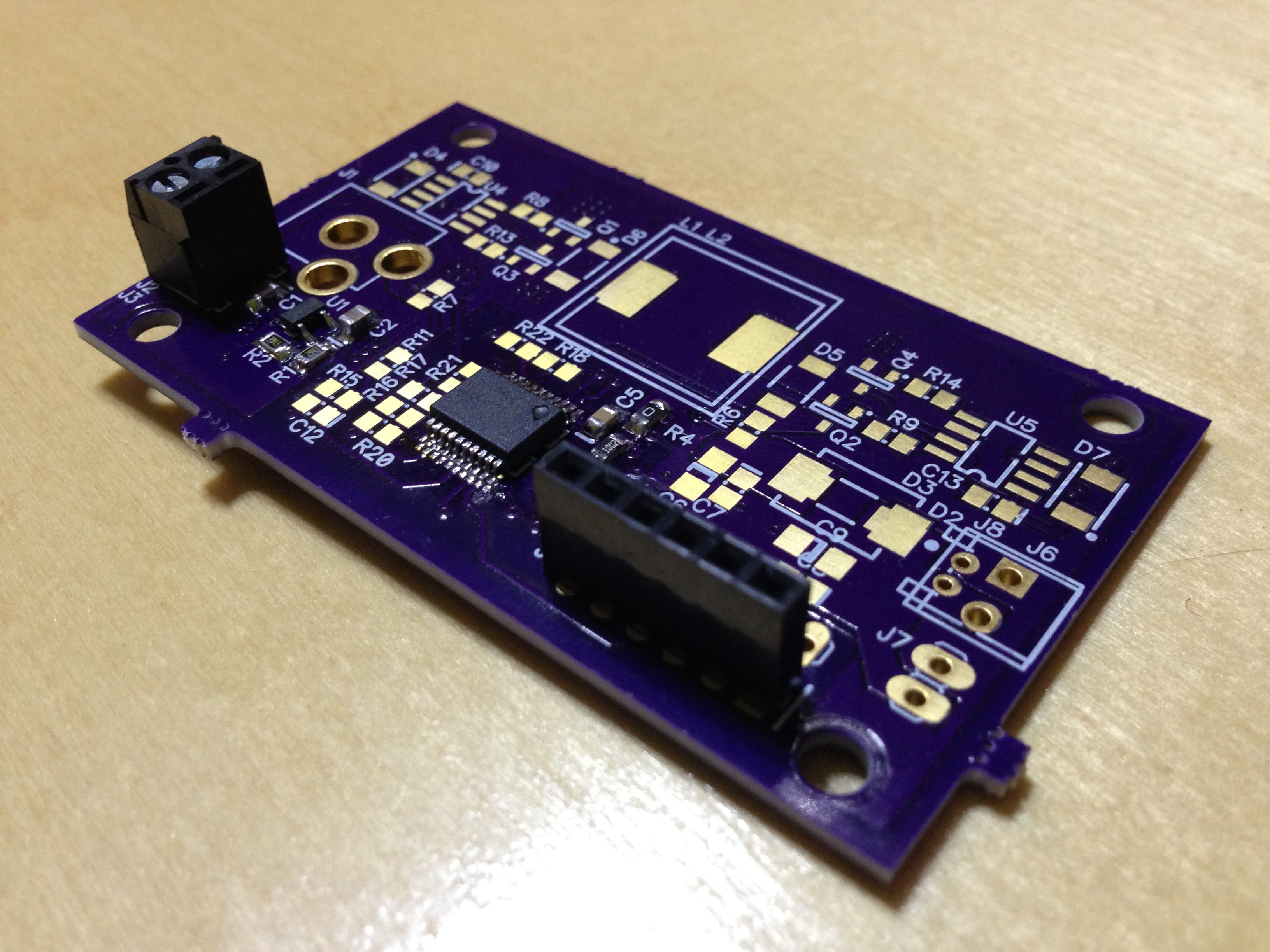

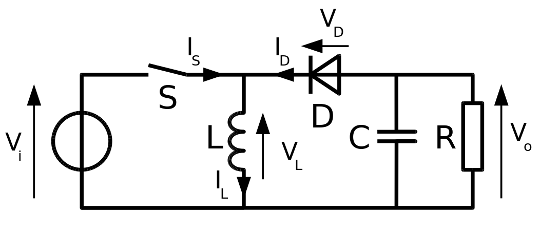
All seemed to be going well until I reached the point where I wanted to add in the makeshift current sensor. I used the schematic below to implement the high-side current sensors (as shown in this AppNote).

But there's a catch. If you look closely at the equation, you'll notice that in order to get a positive gain, R2 must be greater than R1. In making R2 always greater than R1, the circuit above guarantees that the voltage input going into the OpAmp will be greater than the supply powering the OpAmp proper (in this case, VDD) for sense voltages greater than VDD. If this boards was simply a buck converter, this wouldn't be a problem, but since this is a buck/boost converter, we most definitely run in this issue.
What I needed to do was set up a voltage divider that made the voltage stay within the 0-VDD limits and THEN setup a difference gain amplifier. And so this PCB has no current sensors neither on the input (which is almost always above VDD) nor the output when Vout > VDD. Great.
This led me down a slippery slope. The cost of my current solution is within budget but high considering ICs already implement buck/boost functionality at a fraction of the cost (without MPPT control), a large chunk attributed to the smaller inductors made possible by higher switching frequencies and the high level of integration offered by the IC. So I started looking at ways to reduce the BOM count.
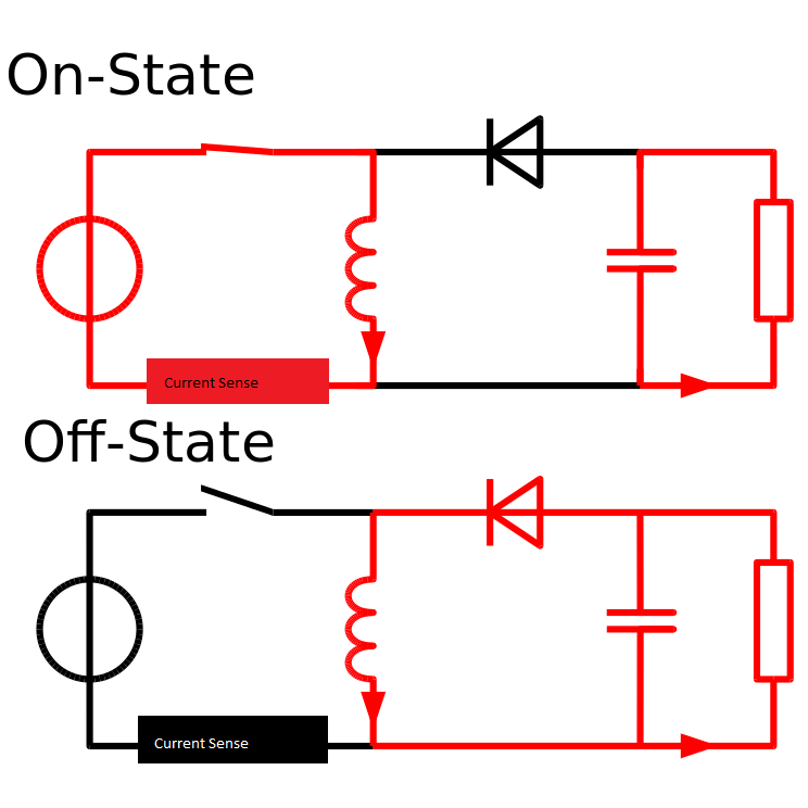
In comes the inverting buck-boost regulators.
It only needs one switch, an inductor, diode, and output capacitor to make it work, and for that, it's brilliant. This design is made more awesome by the fact that a low-side current sensor can be used between the inductor and the Vi source, as that path is only enabled when the switch is closed.
The trick here is to make the high-side switch work. If I play my cards right, I could get rid of the charge pump on the current design (needed to get the voltage up high-enough to drive the NFETs), driving down costs even further. The trick with high side switches is that there are no simple solution, just a series of compromises.
I welcome suggestions/feedback, especially with regards to a high-side switch driver. All I'm seeing thus far doesn't go below 5V, and my target is 2.5V to 18V.
Discussions
Become a Hackaday.io Member
Create an account to leave a comment. Already have an account? Log In.