-
Instruction set
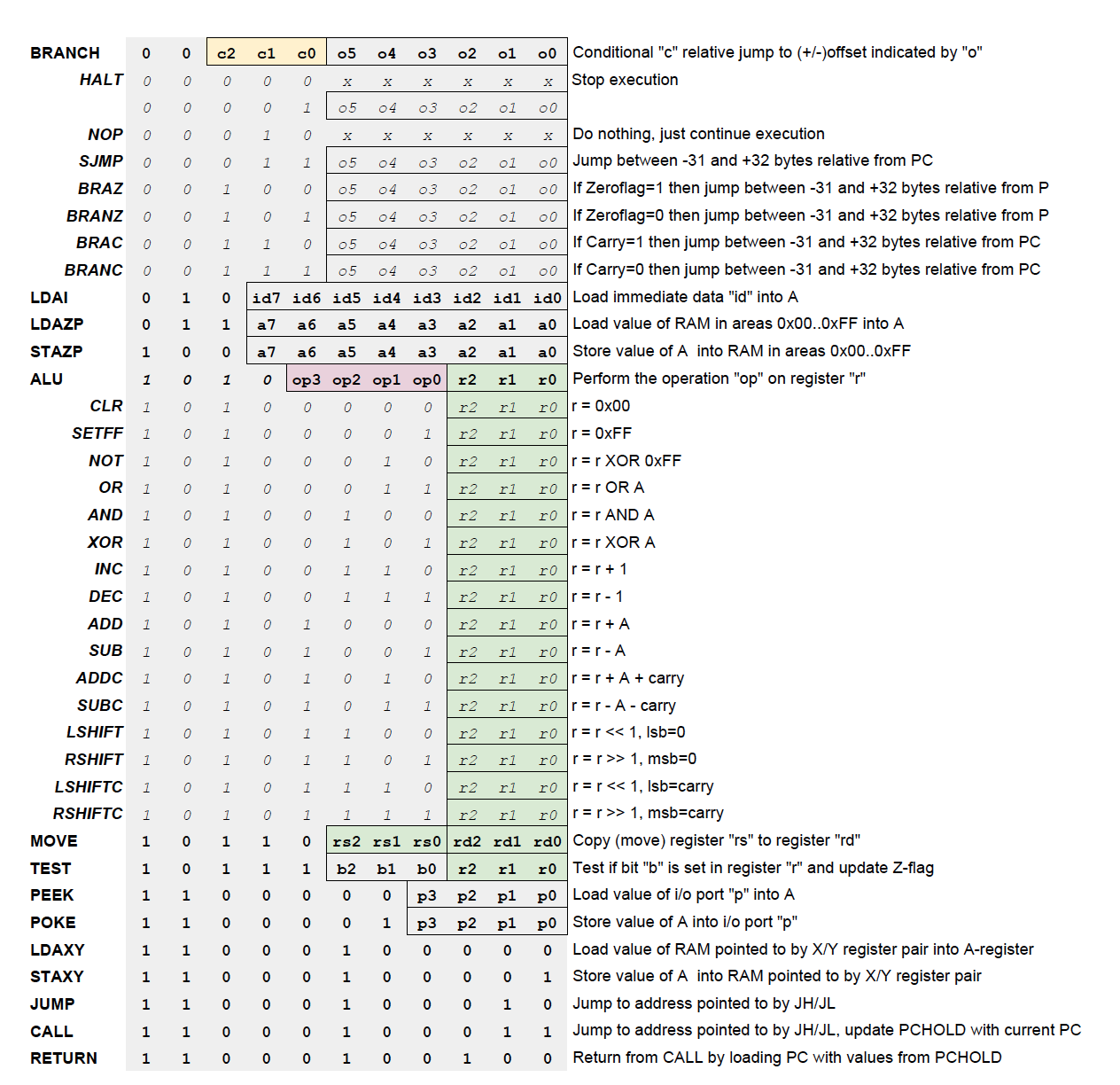
07/17/2015 at 07:46 • 0 commentsI've been thinking a bit of how the overall architecture and the instruction set should look like.
As it looks now I lean towards a Harvard architecture (separate data & program memories) and also separate I/O instructions.
I also want to do a single cycle CPU so each instruction needs to carry its full info/data in a single "instruction byte". This in contrast with for instance a 6502 processor where there are both 1, 2 and 3 byte instructions. For instance DEX=0xCA, LDA=0xA9 0x00, JMP=0x4C 0x00 0x00
To be able to do this reasonably effective on a 8-bit databus I need an instruction width of 11 bits.
I also plan to have 8 registers.A Main working register/accumulator B General register C General register D General register X General register/High memory pointer Y General register/Low memory pointer JH High memory pointer for jumps/calls JL Low memory pointer for jumps/calls In addition to these there will be a 16 bit Program Counter, and a 16 bit Holding register for the Program Counter.
I just realized that I'm missing the SetCarry and ClearCarry instructions in the list below, I'll add them later - too lazy to make another screenshot and upload it again now :-)![]()
-
UART RX Timing board done
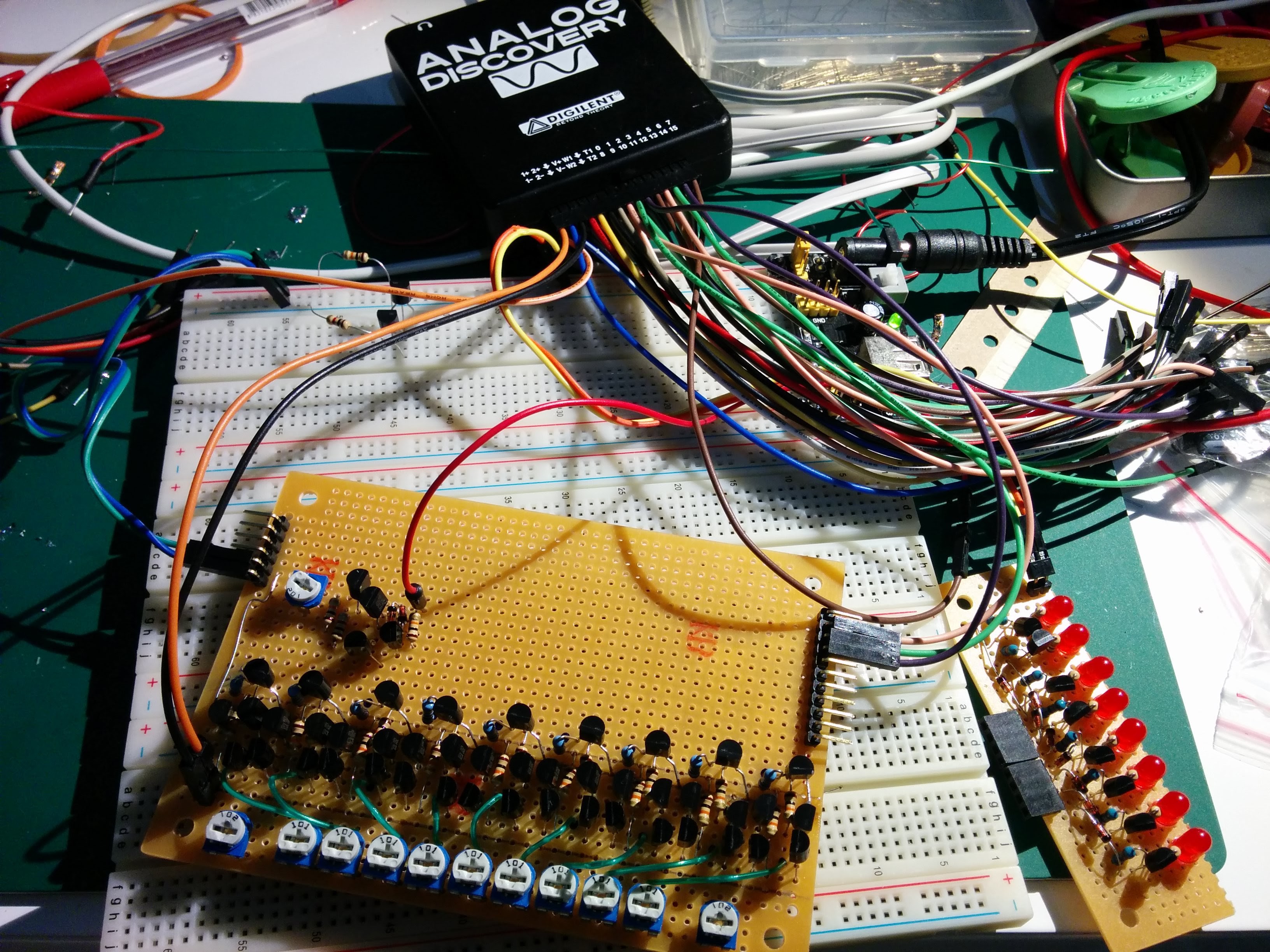
07/16/2015 at 15:09 • 0 commentsThe UART Receiver timing board is now completed, but I haven't tested/debugged the logic part in real life yet. It works just fine in LTspice, and the individual modules tested ok, so unless there's any soldering errors I expect it to work.
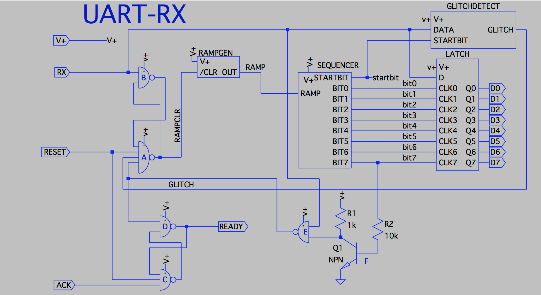
The board holds nine comparators, one ramp generator, one glitch detector and six NAND gates used connected as flip-flops to control the logic and sequencing.The connector at left of the PCB
- RX-data (in)
- Master reset (in)
- Data Ready (out)
- Acknowledge/Data read (in)
- GND & V+
At the right site there's the connector to the D-latch board
- RX-data (out)
- 8 pcs of Latch clocks
- GND & V+
This is a modular view of the receiver (the LATCH-part is on a separate board)
![]()
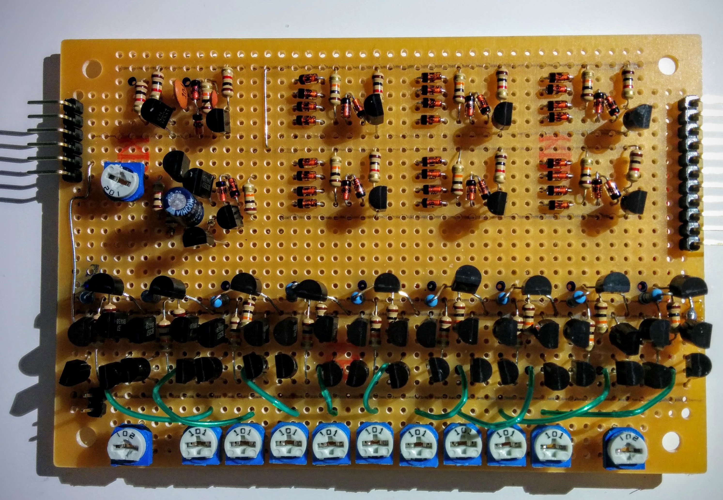
Before the logic wiring - beautiful (or at least ok)
![]()
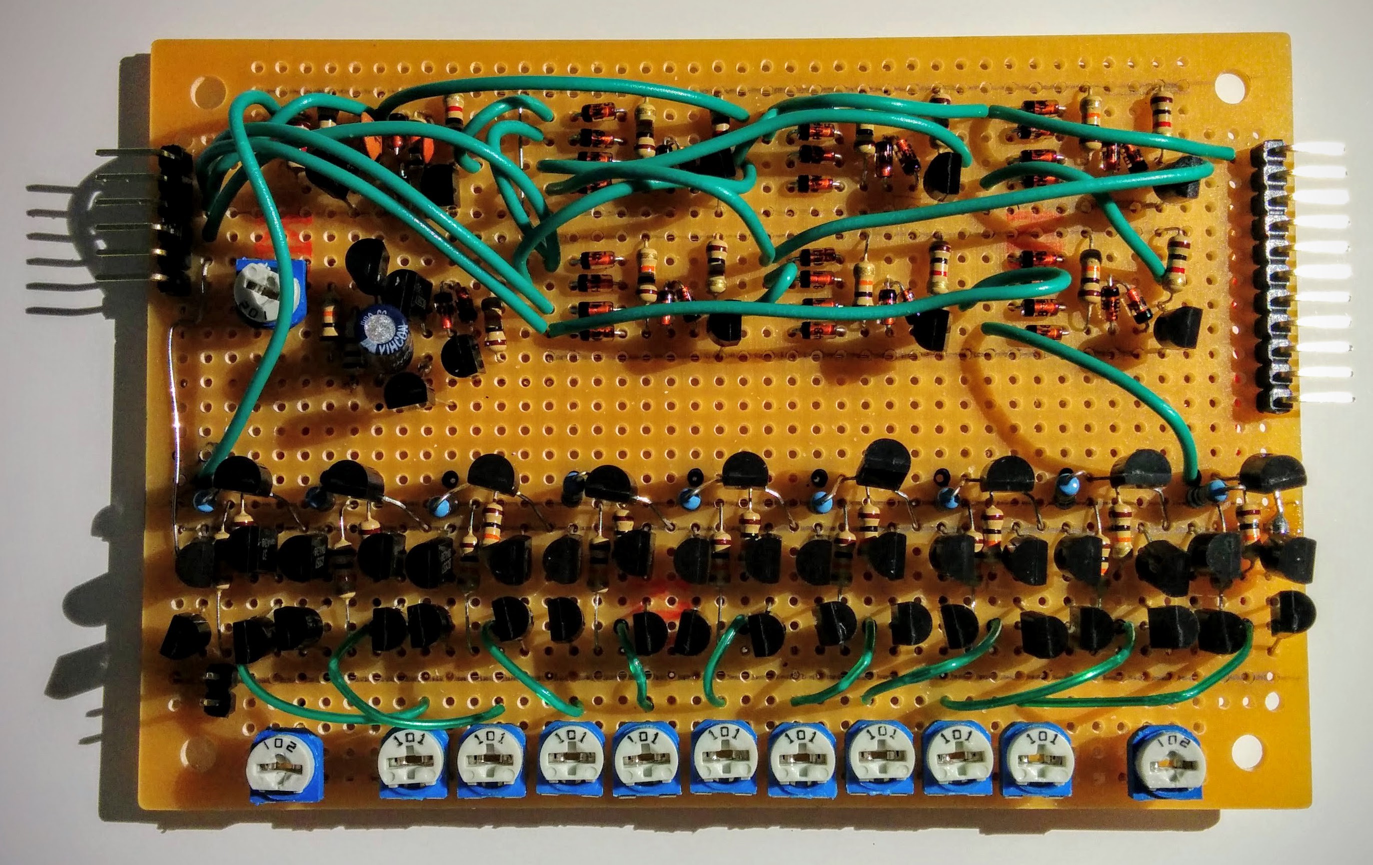
After the logic wiring - messy indeed
![]()
-
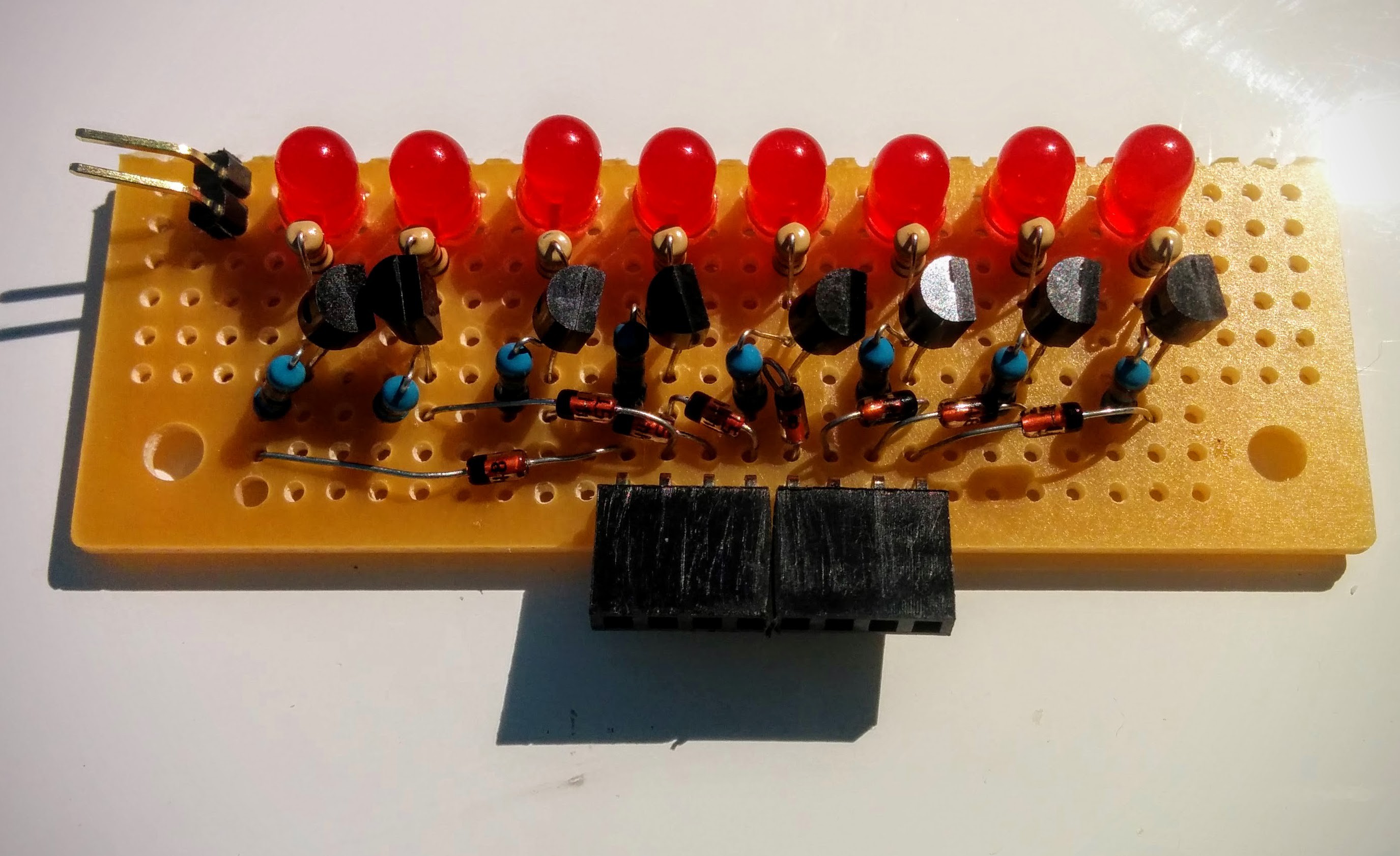
Bus viewer with LEDs
07/16/2015 at 07:45 • 0 commentsAh yes.... I also did a small board with eight buffered LEDs . The inputs are connected via a 680K resistor (to load the DUT as little as possible) and and diode to level-shift the active level up a bit.
The gain of the 2n3904's is enough to drive LEDs decently bright with the minuscule current that passes thru the 680K resistor at 5 volts (minus the diode and transistor junction drops).![]()
-
Testing of comparator-chain
07/16/2015 at 06:02 • 0 commentsJust a quick update of progress:
I've soldered up the ramp generator and the 9 comparators on the UART-Rx pcb.
Testing that it works as it should was really easy using the excellent Analog Discovery from Digilent. Being able to watch the ramp voltage on the oscilloscope and at the same same using one digital output to re-retrigger the ramp at regular intervals and also monitor all the outputs from the comparators with the logic analyzer part of the unit was a marvelous experience.
I'm really happy that I won it in the 7400-logic contest at Dangerous Prototypes some years back. ^_^![]()
-
Added Glitch Detector for RX
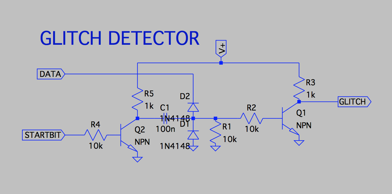
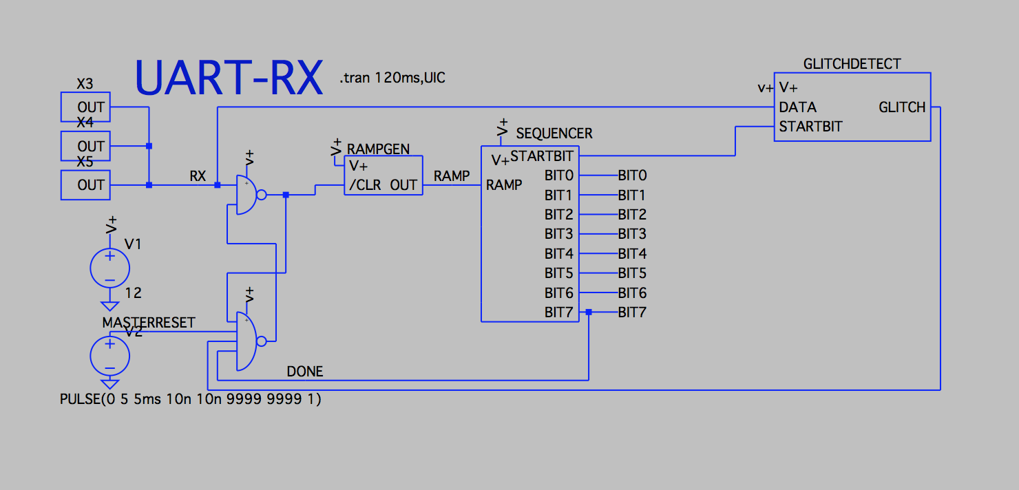
07/13/2015 at 09:36 • 0 commentsMost "real" UARTS have a glitch detector that detects false startbits. I added a simple glitch detector that verifies that the startbit is still active in the middle of the startbit time slot. If the line has returned to idle again then the receiving sequence is aborted.
For this I had to increase the 3-input NAND in the start/stop logic to a 4-input NAND. That was not too much of a hassle, just added one diode :-)
I also added two more TX-fakers to simulate one additional character arriving on the line to see if the design handles more than one character (it does), and also simulate a glitch to test the glitch detector.![]()
![]()
-
Soldering of the Octal D-Latch
07/13/2015 at 02:44 • 0 commentsThis is the result of 2.5 hours of bending, cutting and soldering. Not too shabby I must say...
Since I'm not sure of what voltage I'll run this on I used 1K as collector resistors and 10K as pullups. When the entire board is powered up and outputting low on all NAND gates I measured 420mA power consumption at 12V. That's enough to get the board slightly lukewarm. On 12 volts maybe 3K3 would be a better choice, but currently I really don't care about power consumptionThe parts that went onto the board
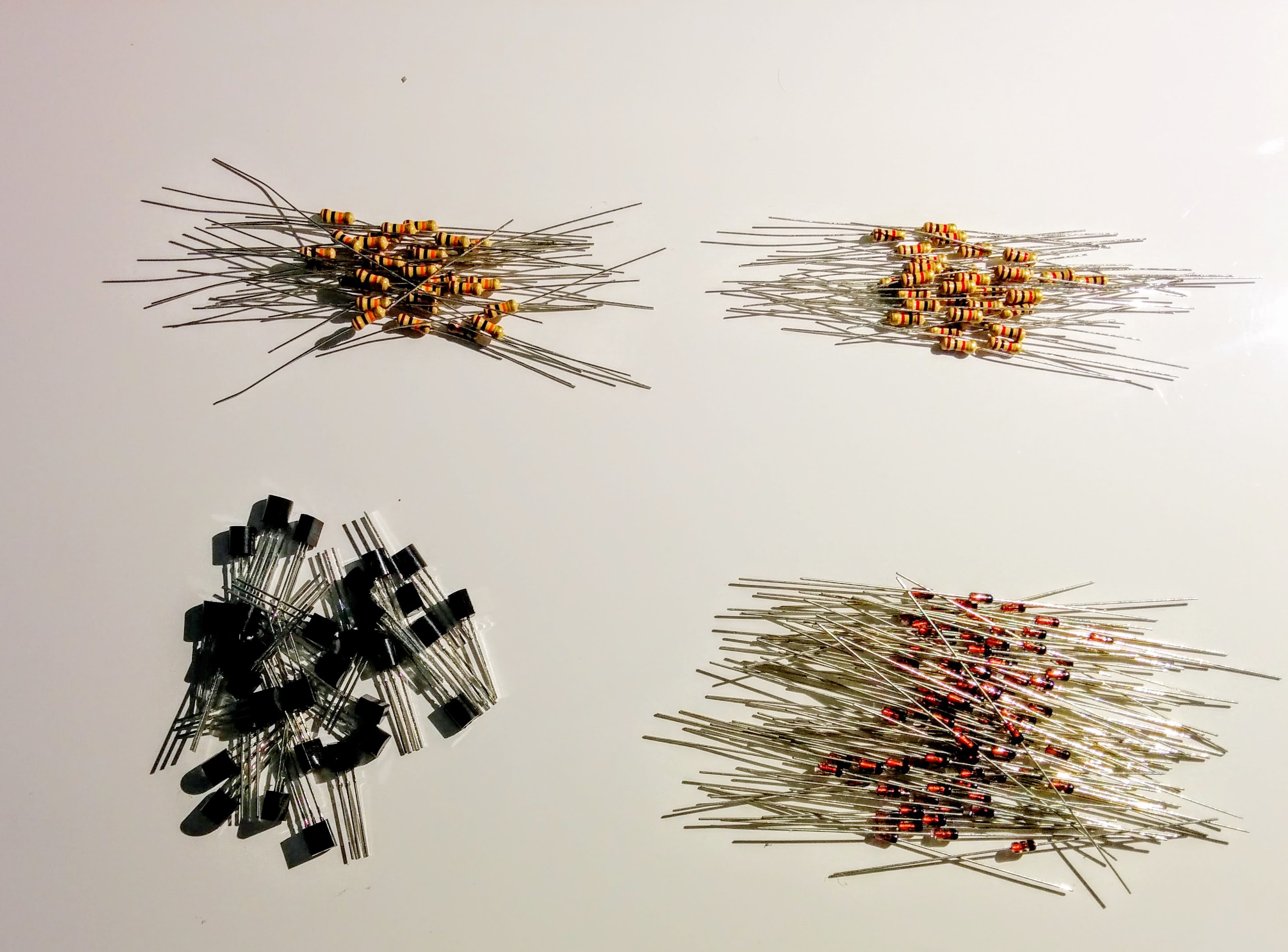
96 pcs of 1N4148 diodes, 32 pcs each of 1K and 10K resistors and 32 pcs of 2N3909 NPN transistors.
![]()
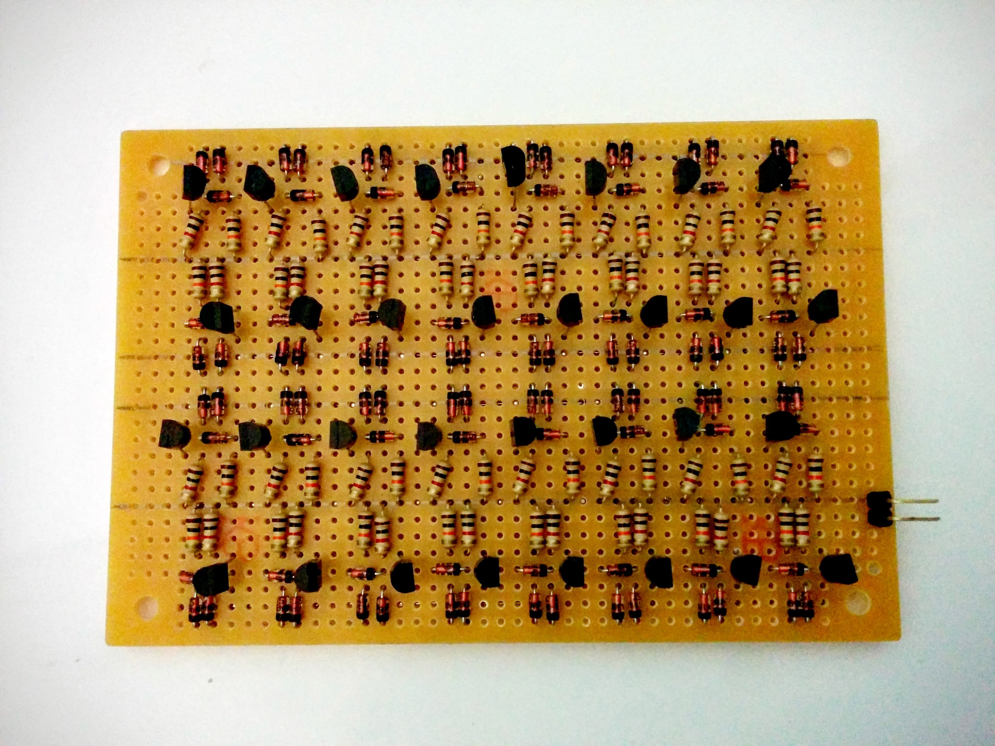
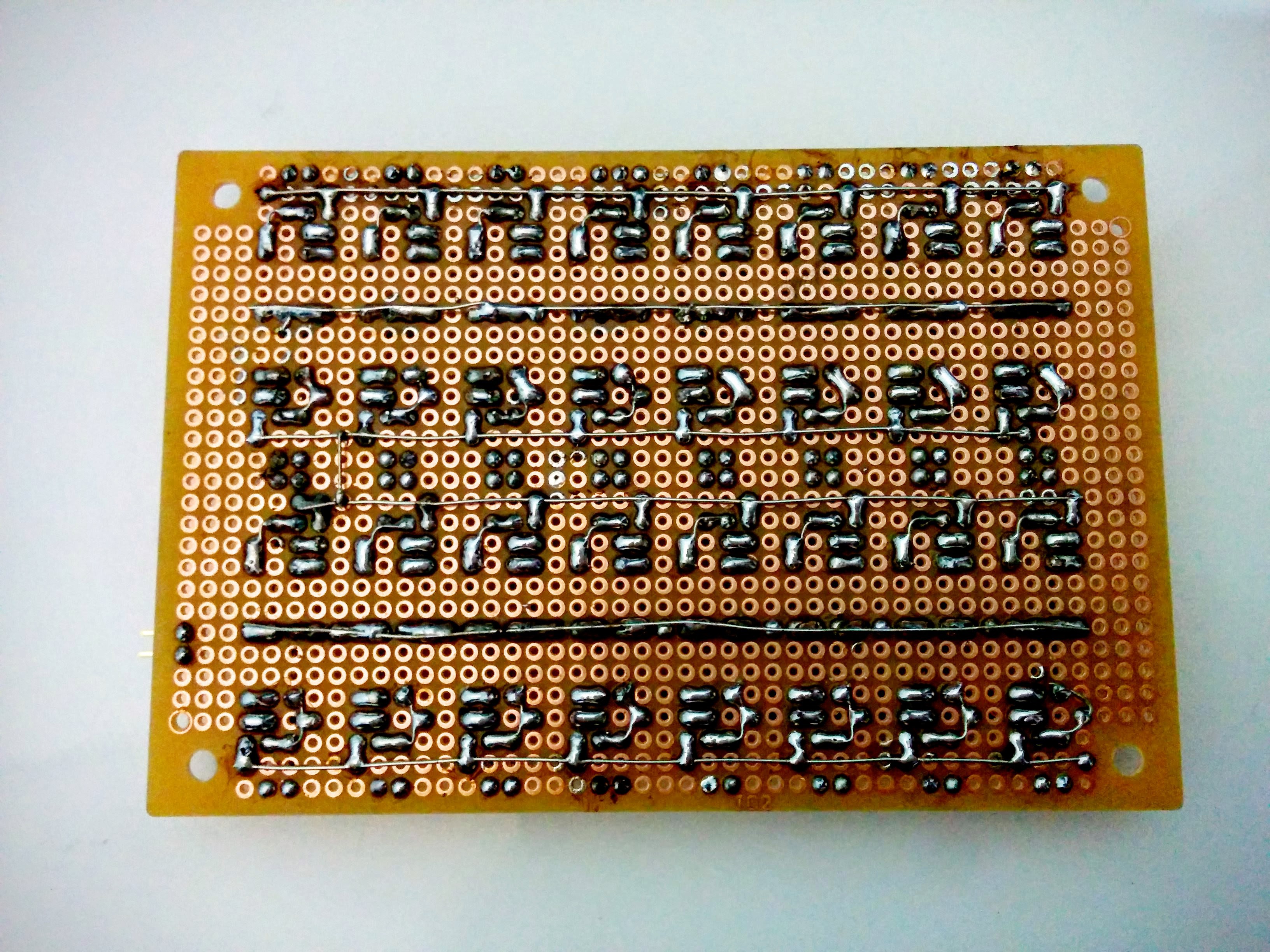
Top and bottom side of PCBThis is the PCB when wired up as 32 individual 2-input NAND gates. Each "column" in the board will have its inputs and outputs interconnected to make them into D-latches, so there will be some flywires.
I also need to hook up the common D- (data) line as well as the 8 clocks and the 8 outputs to pin header connectors.![]()
![]()
-
Received some parts
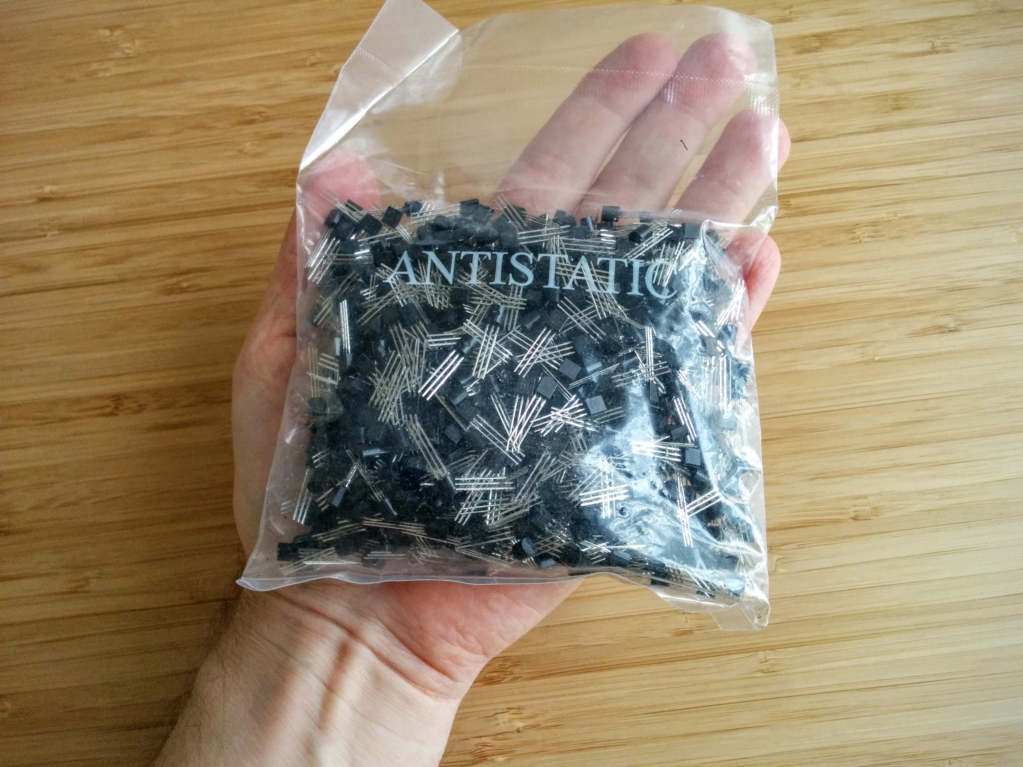
07/13/2015 at 02:21 • 0 commentsThis is how a bag of 1000 pcs 2N3904 transistors looks like. It's quite a handful :-)
Now time to start soldering up 32 NAND gates on a PCB and connect them up to become eight transparent D-latches.![]()
-
Ordering NAND pcbs
07/07/2015 at 14:13 • 0 commentsInstead of trying to wire up dozens upon dozens of NAND gates (which will be by far the most common logic gate in the full design) I routed a small PCB that fits 8 copies of 3-input NAND gates connected to a 4 pin pinheader each. On the PCB there are also common power in & power out connectors .
The PCB is only 20x160 mm (about 3/4 x 6 inch) so they're rather cheap to have made so I ordered 100 pcs of them from Dirtypcbs.
I also ordered a few thousands of transistors and diodes from a local company - I'm sure the parts will arrive long before the PCBs, so I have to start with using my old breadboards :-)![]()
-
UART-RX
07/07/2015 at 04:39 • 0 commentsWell, every journey has to have a beginning so I started of with a relatively simple part of the entire system - the UART.
Currently I have the receiver part of the UART working in theory - it's behaves correctly and can decode an incoming character when run in LTspice.
Next steps would be to prototype some parts of it at solderless breadboards followed by making some PCBs for it.
It will be a lot of transistors when the system is done, the total for the UART receiver is as follows (decoupling caps are excluded from the count)
- 1 capacitor
- 144 resistors
- 137 diodes
- 530 npn and 26 pnp transistors
The LSspice files for the UART is available at :
https://github.com/SmallRoomLabs/aytabtu/tree/master/Spice/UART
AYTABTU - Discrete Computer
After the apocalypse we have to build computers from stuff we can make at home, I.E Transistors, diodes and resistors.
 matseng