Close
0%
0%

FPGA Serial Terminal

Instant-on VT100-style serial terminal implemented in minimal FPGA board, with VGA display and PS/2 keyboard.

Similar projects worth following
When I was a DC/network engineer, I always wanted something about the size and weight of a macbook air that turned on instantly, and would act as a serial terminal with a connector wired to allow using network cables on Cisco consoles, and also to use the display and keyboard as a portable KVM for working on servers. At that time, laptops were relatively expensive and relatively heavy, and something I could just stuff in my bag, and not require a lot of external crap and boot time would have been very useful. If this cost $300 it would have been easily worth it. So 5 years on, I have a little FPGA board, and decided that this would be a good project to learn VHDL.

Original goal was to use the vt100 rom dumps and a 8080 core. New simpler goal is to get a working memory-mapped VGA 80x25x16 text mode, and write a T80-based terminal emulator for it. Stretch goal would be the LCD part - first to replace VGA output with LVDS, then to figure out if the KVM part is possible.

Inspiration material (although not directly useful): The original vt100 technical manual. I didn't know they could overlay video!

VT100 Technical Description

This uses quite a few tricks to get around slow memory, and bus contention between CPU and display controller, like a one-line buffer for the "in-hand" line, and a quick DMA to grab that line. It also describes the very low-level way that double-height and double-width mode worked (it halved the clock for a the line counter, or shifter, logically enough).

I think that I can get away with processing the buffered serial input in the vertical blank, like ZX81 Slow Mode would, and not worry about memory contention or similar.

There's a github repo with my VHDL code in it (and eventually the Z80 assembly too): howardjones/fpga-vt. It's my first attempt at an HDL implementation (or any significant-sized digital logic actually, I'm a software person), so please be gentle.
  • 1 × Altera EP2C5T144C8 mini board Cyclone II FPGA, configuration flash, clock, JTAG and nothing else, on a little PCB.

  • Time Passes

    Howard Jones01/13/2019 at 16:31 0 comments

    After a house move, and office remodel, I'm finally able to look at this project again!

    I did get a cheap Cyclone IV dev board (much more blockram), with onboard RGB565 VGA connector, PS/2 keyboard etc, but then found that it has NO spare GPIO to use for a serial port!

    I also have the Lattice MachXO3 eval board (very cheap, seems nice), but the Lattice software just doesn't work for me on two different Windows systems. The JTAG programmer can't perform a scan.

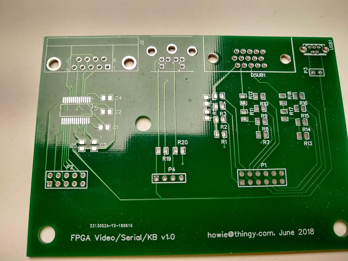
    Somewhere in the last year or so, I did make a small break-out board, to try out JLCPCB and EasyEDA, for a VGA resistor DAC, MAX3241 and PS/2 keyboard connector. I have yet to test one of those - psyching myself up for SOIC soldering. 

    On the VHDL side, I wanted to rework the VGA into a proper CRTC, like a 6845, with timing registers, and multiple clock dividers, to allow for various screen modes. The current VGA is all hardcoded for 800x600, which is not actually the right size for a true VGA text mode. Having a register file for the CRTC would allow the processor to change video modes too, much like a hardware system would. That would open up some potential weird retrocomputing possibilities, like Videotex, or maybe PLATO.

    If I can get a working MachXO3, or back to the Cyclone II, the two immediate goals are serial from the MAX3241, and programmable video timings.


  • Small update

    Howard Jones11/03/2015 at 14:30 0 comments

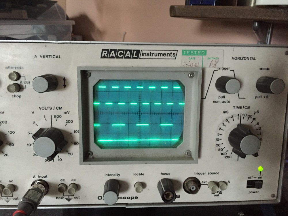
    I've got some standalone serial and VGA breakout boards now, so I decided to try moving over to the smaller EP2C5 board that was the intended target. This has a 2-bit resistor DAC per RGB channel for the VGA, and a MAX232 chip for the serial, so it can talk to the rest of the world. Except that it doesn't, even to my buspirate. So I (literally) dusted off my 1980s oscilloscope to see if I was even generating the right kind of thing...

    Where it turned out I was out by a factor of 10 in my clock counting process, so running at more like 960 baud instead of 9600. With that fixed, I can see bits on the scope, but obviously not the right ones as the PC and Bus Pirate both still show nothing. The top trace is the 9600 baud clock, and the bottom one is the transmit line. I've just got a 10 bit buffer being rotated to send a start, ASCII 'A' and stop bit, currently. It might be time to get a modern DSO (and win back some bench space), because I can't really get this to trigger nicely to show a full word.

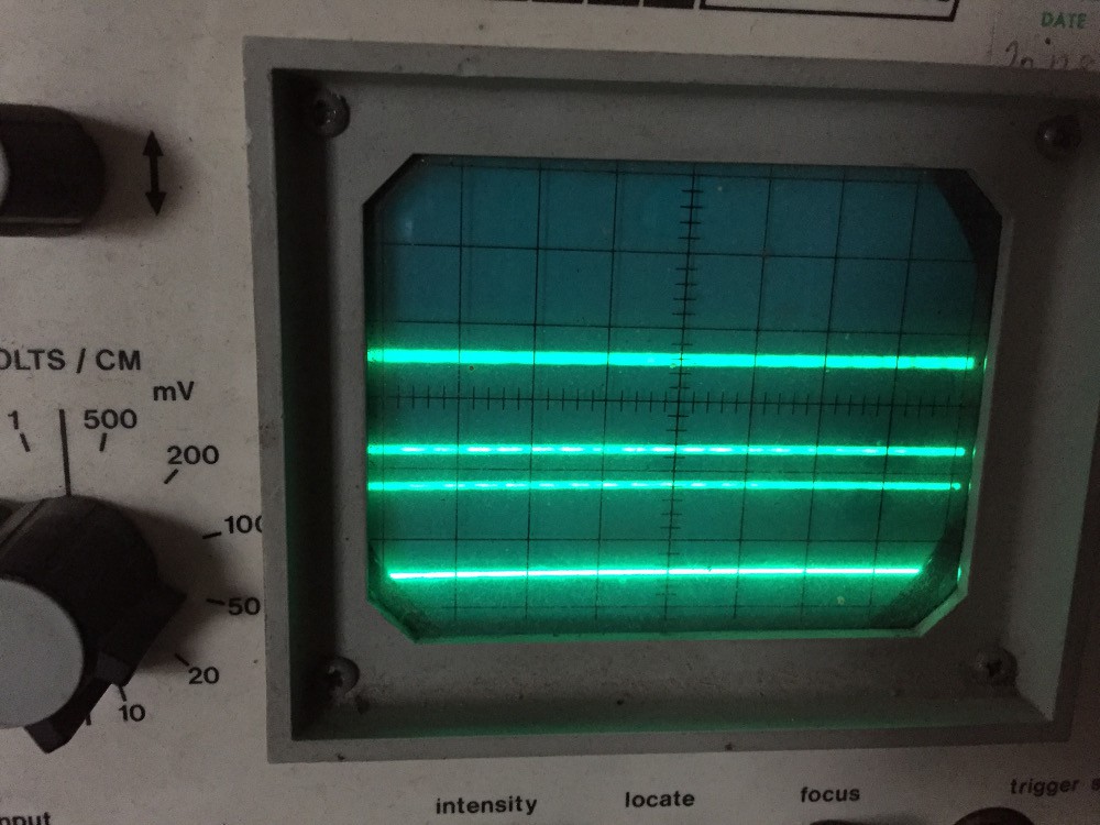
    While I was fooling around with the scope, I also noticed that the resistors on my VGA DAC aren't very well chosen. The scope can't show an actual signal (it maxes out at 10MHz, I think, and the VGA dot clock is 50MHz), but I'm pretty sure these 4 lines should be evenly spaced:

  • Hardware is slower

    Howard Jones10/10/2015 at 11:18 2 comments

    Things have slowed down a little with the terminal - partly due to the need to actually create something physical next. I've decided to learn how to etch my own boards, and make a little breakout PCB for the serial, VGA and PS/2 connections. Partly because I'll need them for the final target FPGA board, and partly because the dev board I do have seems to have something strange with the serial port. With my bus pirate, I can see traffic from the uart on the right pins, but somehow that doesn't actually appear on the db-9 connector at the edge of the board, and hence doesn't reach the PC. So I'll be using some GPIO pins and a breakout to make a serial port that I know for sure how it works. It looks like I will need an external 1.8432 MHz oscillator to get selectable baud rates, too - the onboard PLL can't generate that from the 50MHz system clock. You can get some serial clocks (e.g. 19200, 9600) OK, but I'd rather have the UART baud rate register work properly so it's all software-selectable!

    On the HDL and software side, there's a makefile to build the z80 firmware and the FPGA bitstream now. I finally fixed the annoying whistling noise from the dev board, and the Z80 does some more self-test now. I really need the I/O to get further - keyboard in, and serial i/o - so I've got a cheap UV exposure box ($15 from ebay, intended for curing nail varnish), a little chemical kit, and the free version of diptrace. Time to ruin some 2-inch squares of FR4...

  • Address decoding II - electric boogaloo

    Howard Jones09/21/2015 at 22:25 0 comments

    I wrote some quick assembler loops to blast the display RAM with characters, and it was strangely lumpy. I eventually figured out that the counter that I was pushing onto the stack to make room for another counter (one for rows, one for columns - the handy Z80 loop instruction (DJNZ) only works on a 8-bit register) was not actually being saved anywhere. So the lumpiness between bursts of update was while we waited for the Z80 to go all through the rest of the memory map trying to write before coming back to display RAM.

    With that fixed (same error as the display RAM decoding, d'oh), the stack works, and the screen updates are really fast. I also got my dev board's LEDs hooked up to a Z80 I/O address so that software can signal status.

    Finally, I started on a build script. It will turn into a makefile, but for now a batch file will assemble the Z80 ROM, pad it to 4K, convert it to intel-hex and tell Quartus to rebuild the FPGA image without synthesis. That all takes about 4 seconds instead of much longer for VHDL hardware changes.

    I've also been looking around for a nice small laptop that's old enough to be worthless to normal punters, so I can get a cheap one on ebay. It needs to have a known LCD screen and either a documented or brain-dead keyboard ideally. I like Lenovo keyboards, so perhaps an old Thinkpad X? Failing that, my beloved 12" Powerbook G4 might be a candidate.

    Back to the serial port now...

  • Small victory at last

    Howard Jones09/19/2015 at 17:29 0 comments

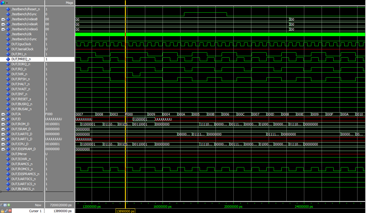
    I fired up the project in ModelSim, and added all the Z80 and memory-related signals to it. From there I could see that memory requests in general were working OK, and could watch the Z80 pull bytes from ROM in low memory. I could also see where we got to the "LD (HL),A" instruction, that should update the display RAM at F000. F000 turns up on the address bus along with MREQ' and WR' and 65 on the data bus (a letter 'A' in ASCII). However, the chip select lines for the display RAM stay at 1 (off, it's active-low) and the request goes to the ROM instead.

    Here's a picture of the problem. I think this stuff is really cool! Because your design is 'soft', you get a infinite-channel logic analyser for free... the DUT/A line is the system address bus, and DUT/DISPRAMCS_n is the display RAM chip select, with the others above it. At the yellow cursor, the Z80 has just asked for F000 - the actual write comes a clock later (clock at the top, WR_n a few lines below). Neat side note: You can also see the built-in Z80 DRAM refresh mechanism happening, which is why the address bus keeps jumping backwards and forwards - it's two sequences. One is driven by the Program Counter, and is fetching instructions, or data from memory with MREQ low, and the other is cycling through a 7 bit counter with RFSH low, to help you keep your DRAM refreshed. It does this while the rest of the processor is thinking about the current instruction, so the bus isn't required for memory or I/O access.

    Anyway, knowing that the issue was with decoding, I noticed that I was comparing a 5-bit value to a 4-bit value for the display ram address decoding - something that the VHDL complier normally complains about - corrected that, and we were up and running!

    For about 20 seconds.

    Because now the address decoding is working, none of the RAM is optimised away, and the compiler has noticed that I still have dual-port, dual-clock RAM. Apparently, the same-size data buses isn't enough to fix it. So I lied - I told the system that I had the rev B fixed silicon. I actually have no idea if I do, because I can't figure it out from the label on the chip, but the symptoms are "possible memory corruption in certain circumstances", and since I have (mostly) one writer and one reader, I'm hopeful that I'll be OK. There is another workaround, but it uses twice as much blockram, and I don't have that to spare.

    So the final exciting result:

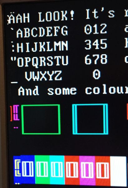
    "AH LOOK" used to be "OH LOOK", and the "A" was put there by the Z80 software! It's not astonishing, but everything is talking now. Also, you can see the column-9 extension stuff working in the box graphics below it, to produce continuous horizontal boxes.

    On to some slightly more advanced software to test i/o via the UART, a bit more virtual hardware to generate the 1.8432 MHz clock that the UART wants to generate baud rates, and some real physical hardware (MAX232 for now since I have one handy) to get the serial port to the right voltages to talk to other devices.

  • Read Only

    Howard Jones09/18/2015 at 22:21 0 comments

    VGA side now works with 8-bit fetches from display RAM, and the design synthesises again! Also, fixed a timing issue with the Flash attribute where it flashed a character early, and added in the logic for extending box-graphics characters so they join up.

    I also finally slowed down the Z80 clock enough that I could see A11 toggling away. Yay! Then I found that I can edit the contents of FPGA blockRAM (including ROMs, but not dual-port RAM) while the system is running, using the Quartus JTAG tools, so I was able to prove to myself that it's really fetching instructions from the ROM by moving the JP 0000 nearer and further from the end - A11 flashes faster, and not at all if you put the JP instruction in the lower 2K of ROM. So that's cool. I found the option to rebuild the bitstream with new memory images without changing the logic too (3 seconds vs 2 minutes), which will be helpful for the software side of things.

    However, the 9 bytes of real code in the ROM was supposed to write a character to the display RAM, and that isn't happening. In fact, the synthesis tools seem to be optimising the 1K (other) RAM away altogether, so something isn't quite right there. I suspect it's with the address decoding logic (a funny mix of active-low Z80 signals and active-high signals for the IP memory), so it might be time to get the simulator going again, although with a full CPU in there it might take a while to run!

    Next steps:

    1. Writeable RAM
    2. Figure out an OK development environment for writing Z80 assembly and/or C.
    3. Get the UART hooked up to the outside world and prove that it reads/writes, too.
    4. PS/2 interface is next, I guess.

  • Hiccup

    Howard Jones09/14/2015 at 22:06 0 comments

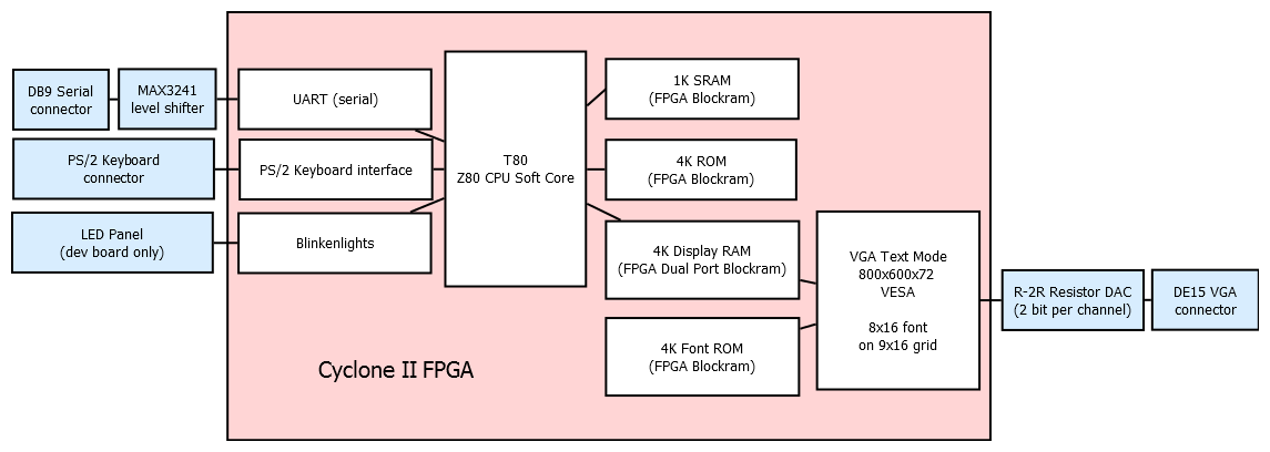
    I patched in the T80 processor, a 4KB ROM (empty apart from a JP 0 at the end), a 1KB SRAM and a 16450 UART today. It took surprisingly little fighting to get it to synthesise, copying mostly from the "DebugSystem" toplevel supplied with the T80 tarball, although when I started to connect up the 'A' port of my dual-port display RAM, it turns out that the Cyclone II FPGA I'm using doesn't actually support dual-clock, dual-port blockram, even though the Altera software initially says it does! [*] I also found yesterday that I can't create PLL components, even though the chip does have two clock managers, which is a problem for the pixel clock change.

    New problems then:

    1. Find a way to prove the Z80 is actually running. LEDs on the A11/A10 lines don't appear to be cycling, with a roughly 1.5MHz CPU clock. Maybe I need an even slower clock. Once I can see the bus moving, I'll add the row of blinkenlights on the FPGA board as an I/O port.
    2. Figure out how to get data from the Z80 into display memory. Could this be using more I/O ports and some registers to track the cursor and write data? The screen doesn't *have* to be memory mapped...
    3. Work out the counters to centre and mask the 80x25 display in the 800x600 screen, since I'm apparently stuck with that.

    Good news is that everything (CPU, UART, VGA, misc) fits into about 2700 LEs, assuming that Quartus isn't optimising anything away. Also, the flash attribute works as expected.

    Testing the UART will require a working CPU, and also the external interfacing that I've been putting off wiring up. That will also get me 16 colours though, and a PS/2 port.

    [*] Specifically: dual-clock, dual-port with different sized ports. I use 8-bit on the z80-facing port A, and 16-bit on the VGA port B, to fetch the character and attribute bytes in one shot. There is probably time to do two 8-bit fetches there.

  • Attributes and Display RAM

    Howard Jones09/13/2015 at 21:01 0 comments

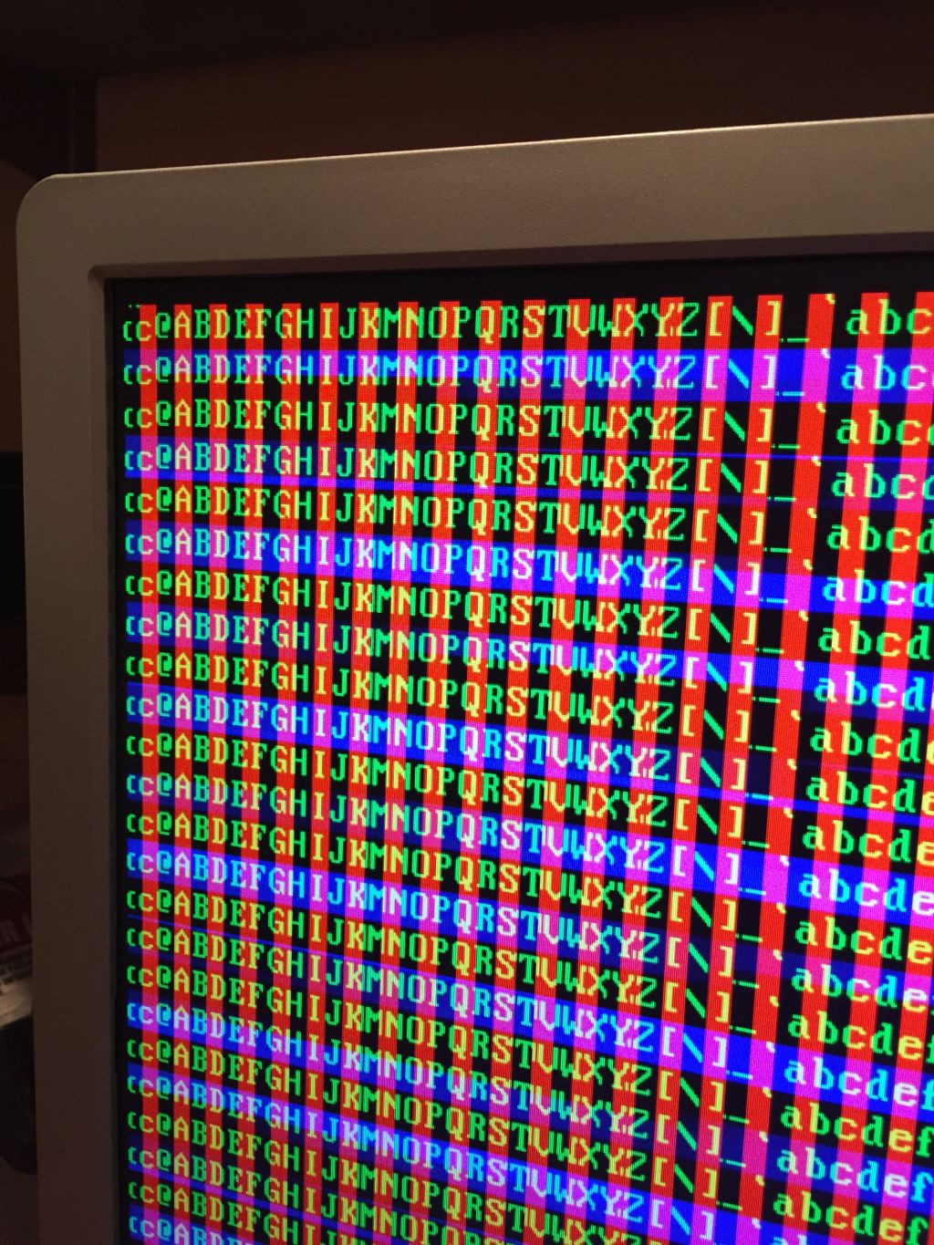
    Data is fetched from display RAM now, and the attribute byte is decoded correctly. I used an ANSI-art editor in DOSBox to produce a test screen and saved it as a .bin file, which is a VGA memory dump. The FPGA tools don't really distinguish internal between ram and rom, so it's perfectly OK to have RAM but preloaded with data at startup. The display RAM is full-dual port, dual-clock, so the Z80 can live in its slow 4MHz 8-bit world while the VGA side of things grabs 16-bit words at a time. For updates from a serial port, I'm not too concerned about tearing etc. The screen is showing fg and bg colour changes, and a full-ish ASCII character set. Attribute decoding worked first time, pretty much.

    There's no bounds-checking on the display though, so outside of the 80x25 main area, there is random overflow/wrapped data. I should be suppressing before the first real character, on the left, and after column 80 (81). A real VGA textmode runs in 720x400, not 800x600, so I have a bunch of extra space on the screen. Unfortunately, without switching to using external RAM, I can't really use it to display anything, so it'll most likely be blank, or I'll figure out how the Dynamic Clock Manager works to generate the right 35.5MHz dot clock for 720x400@85.

    You can also see where I haven't yet implemented the column-9 extension stuff for box graphics.

    Still haven't figured out the whistling noise. Tying the relevant I/O pin to a constant-0 output has not helped.

    Next steps:

    1. column-9 extension
    2. test flashing
    3. bounds-checking and/or resolution change
    4. CPU!

  • Github

    Howard Jones09/11/2015 at 10:12 0 comments

    There's a github repo with my VHDL code in it (and eventually the Z80 assembly too): howardjones/fpga-vt. It's my first attempt at an HDL implementation (or any significant-sized digital logic actually, I'm a software person), so please be gentle.

    Today's software vs hardware lesson: I already knew this at the back of my head from writing 68k assembly years ago, but I noticed that my Logic Element usage on the chip jumped up from 200 to 1600 some time recently. Looking at the RTL, I found a massive array of logic gates eventually feeding into the 'flash' flag (which is ANDed with the actual pixel to decide if the foreground or background is shown on a flashing character). Why? because I have a counter to count frames ("jiffies") and used that to decide if the cursor or character flashing flags need to toggle. I wanted them to flash at different rates so that the cursor wouldn't get lost. My rates were "mod 27" and "mod 36". Switching to 24 and 32 saved 1400 LEs, or about a quarter of the entire FPGA (roughly 5000 LEs on the target board, 8000 on my dev board).

  • Slow progress

    Howard Jones09/10/2015 at 21:14 0 comments

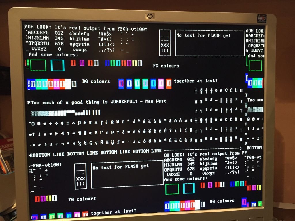
    Actual characters on an actual screen. What I thought I had worked out ages ago was not really correct.

    This is 800x600 @ 72Hz SVGA mode, with 9x16 character cells and 8x16 font. The red bars are 8 pixels wide which is why they drift out of step with the characters. On a VGA screen, line-drawing characters are extended into column 9, to allow you to draw continuous boxes, so column 9 of the character is generated from column 8, if the character is within particular ranges, otherwise you get the spacing between characters.

    The actual character grid will start in further from the edge of the screen to allow time for the first character to spool up (fetch from screen ram, fetch from font rom, and interpret the attribute byte).

    Next steps:

    1. Wire up the 2-bit R/2R VGA DAC and a new DB15 connector - currently the dev board's built in VGA port uses only one pin each for R,G,B and I need 16 colours, not 8. (Final target is a smaller board with no fancy I/O anyway)
    2. implement attribute decoding, and a latching register for the fg/bg colours to latch on the new character (after being prepared during the previous one).
    3. implement the selector logic for fg vs bg with flashing (flashing is already there).
    4. implement screen RAM with altsyncram - I already have some ANSI gfx in screen RAM format to test with.

    At that point, we should be ready to hook up a CPU!

    Also, on the dev board I'm currently using, the buzzer produces a high-pitched whistle, despite nothing being assigned to its I/O pin. It'd be nice to not have that. I also just noticed that C, L and U are missing from the character set below... probably not a coincidence that there's 8 characters in between each missing one.

View all 10 project logs

Enjoy this project?

Share

Discussions

Lee Hart wrote 06/03/2024 at 16:49 point

Wow! This is an impressive first FPGA project to tackle. Kudos for sticking to it for so long.

I see it has a Z80 core. Could it be built with a real Z80? I like the idea of a vintage terminal built with vintage parts. I designed and wrote software for a Z80-based terminal back in the 1980's, so such a project would give me a chance to re-use that knowledge.

I solved the Z80/video contention problem by noting that the Z80 only reads/writes data RAM during its T3 cycle. With fast RAM, I could multiplex the address between the Z80 and video a half the Z80's clock speed to neatly interleave the accesses.

  Are you sure? yes | no

Kuba Sunderland-Ober wrote 02/18/2024 at 20:24 point

Display memory contention was a problem back when memory was expensive. In many an FPGA today, it's easiest to have two screen buffers, one for random access from the CPU, another for display. Sometime during the vblank interval, the the random-access RAM gets copied to the on-screen RAM. This can be very fast - using a wider data path than the CPU uses, and a much shorter end-to-end delay. So while let's say the CPU core may need to run at CLK/2 or lower, the RAM copy can go full blast.

  Are you sure? yes | no

legacy wrote 02/06/2020 at 17:56 point

I cannot see the assembly/C file for the VT100 implementation. Is it possible to see it? thanks

  Are you sure? yes | no

Howard Jones wrote 02/21/2020 at 08:45 point

I haven't written it yet!

  Are you sure? yes | no

zpekic wrote 01/08/2021 at 18:23 point

First, congrats for a cool project! I use a scaled-down variation of the same idea to debug my FPGA-projects. I generate simple TTY output from the device as debug log stream, intercept that is a simple "terminal" (which recognizes only printable ASCII + CR + LF + CLS) which writes to a text video RAM. A simple 640*480 text mode VGA displays it. The "terminal" program is in microcode, so it can run at speed limited mostly only by the serial output. Here is a description, but I used similar in other projects too:

https://hackaday.io/project/172073-microcoding-for-fpgas/log/178441-proof-of-concept-tty-to-vga

  Are you sure? yes | no

greenaum wrote 08/19/2017 at 19:18 point

Just a thought... late though it may be and completely not what you were planning...

But what about including a small LCD display in your terminal? Or, as an option, maybe Bluetooth to a mobile phone screen? With a Bluetooth keyboard. So your device would be a box that plugs into a serial port (with whatever connector) and produces Bluetooth connections for the display and KB?

Or if you don't fancy using a phone (I can see why, aesthetically, plus it's another barrel of monkeys to worry about), just go with an LCD plus a Bluetooth keyboard. You can get teeny Bluetooth keyboards or full-size ones, with a couple of options in between.

You could also stick a USB or PS/2 port on your device to interface with any handy PC keyboards lying around. Are modern keyboards still dual-mode USB / PS/2 ? The keyboard detects which connection, I think, through which pins are connected to what. So you could have a "USB" socket that actually only speaks PS/2, with the appropriate pin arrangement. The reason behind that being that PS/2 is much simpler to interface with.

Just ideas that popped into my head. Because if you're gonna use a laptop in the first place, you may as well just use a USB serial-port dongle and terminal emulator software. It's not instant-boot of course. But if you're gonna put up with all the nonsense a laptop brings, it seems the sensible way. If you're gonna build your terminal from scratch, I'd do away with it. I think using a laptop just for a screen and keyboard is a waste, too bulky and too heavy. Better to make something portable, but still convenient to use for debugging, if not perhaps all day long sessions.

Then you'd only need a monochrome LCD. Nice, low-power, cheap, clear picture. Optional backlight.

Also for a laugh, maybe a "stretch goal" if there's enough memory, a port of a small BASIC interpreter? Or your own scripting language, or at least macros. So you could automate certain common tasks, with BASIC of course being able to access the serial port.

Or FORTH, if you're a nutter!

  Are you sure? yes | no

Howard Jones wrote 08/19/2017 at 21:32 point

What nonsense does a laptop-shaped item (thinking macbook air size) that doesn't have an OS or storage bring? I can count the number of bluetooth keyboards I have run across, ever, on one hand... However, I can leverage laptop manufacturers buying power to get a display and keyboard that are cheap and easy to replace (roughly $10-20 each if you pick well). If anything, I'd want the display/keyboard combo to be able to act as an PC monitor and keyboard as well, for the on-site visit where you don't have a KVM console or crash cart. Once the software is sorted, my plan was to move on to a LVDS LCD and a non-PS/2 dedicated keyboard (got those waiting already), in a 3d printed chassis. Finally from there to a machined chassis (think unibody). Definitely agreed about the basic/macro language though :-) If it ends up on a Cyclone III or a Lattice MachXO2/XO3 (all with more block ram), or with an external RAM, then for sure.

Of course, it also needs me to finally unpack my project stuff again after moving into a new office/workspace :-)

  Are you sure? yes | no

Hacker404 wrote 10/13/2015 at 08:05 point

I am just reading up now. That dual port BRAM will make the task much easier. I am guessing you are using an EP2C5 for video and glue. How do you get the Z80 to work with it. The datasheet doesn't say the EP2C5 is 5 Volt tolerant? and the FPGA seems too small for a soft Z80!

I am using a EPM570 CPLD - 490 LE's. I first did the HSGVA in a xilinix XC9572XL CPLD 72 macro's so not much is needed for the video part.  

  Are you sure? yes | no

Howard Jones wrote 10/13/2015 at 08:18 point

There's plenty of room for a soft Z80 actually! I have a soft Z80 (T80), 2 UARTs and my VGA text mode implementation in about 2500 LEs (roughly 50% of the EP2C5). The remaining bits (PS/2 keyboard interface, mainly) are not going to use much more.

I used all the BRAM though, to avoid having to interface external memory. Time will tell if 4K is enough ROM for the terminal - I think it should be. If not, I can win back another 2K by being "authentic" and only having a 7-bit ASCII character set, or adding the external SRAM, and probably an SPI flash to bootload from.

If it was just the VGA, it would definitely fit in a CPLD - that was only a few hundred LEs, although I guess it'd be a bit more to deal with external memories.

  Are you sure? yes | no

Hacker404 wrote 10/14/2015 at 09:38 point

Ok LOL, You may be a VHDL "learner" but your way ahead of me. I am still playing with CPLD's. I have some FPGA here - a Papilio One - 500k that I have played with - as in just writing simple code. 

So it seems that a soft Z80 will fit into a couple of thousand LE's or LC's or what ever they are lol. I don't yet understand the 'lingo' so I think of things as being a number of 'registers' that dictate the number of states a state machine can have.
 

Anyway the xilinix chip I used had 72 'registers' and combinational logic. It is based on the ancient 22v10 chips of the past. SVGA fits into about 30 registers. I don't know how that relates to 2500 LE's but that many seems very high in number.

  Are you sure? yes | no

Howard Jones wrote 10/14/2015 at 10:45 point

I think Xilinx, Altera and Lattice all use different names too, to make it harder :-)

I've never used CPLDs, but my understanding of it is that CPLDs have lots of gates (combinatorial logic) but not so many flip-flops/registers, and FPGA have many more registers, as well as just being bigger.

Check out Grant Searle's Multicomp project - that's what got me interested in the soft CPUs. The amount of code needed to glue someone else's CPU in is fairly small. Especially if you already know a bit about the real CPU - I dabbled with z80 hardware many years ago. I'm pretty sure that your Papilio board has plenty of room for 80s-style micros like the C64 or Spectrum (and much more RAM than the little Cyclone I have - 40 whole KB).

  Are you sure? yes | no

Howard Jones wrote 08/13/2015 at 11:10 point

It does, just. 13KBytes of M4K blocks. The VGA font is 4K, the display is 2K (80x25) and the attribute bytes are another 2K. I'm somewhat concerned about writing a terminal emulator in 4K ROM and 1K RAM though :-) I do have an SRAM chip somewhere, if it comes to it, which it probably will. I think at that stage I'd add an external serial flash too, so that the on-fpga ROM just has a bootloader to stream the real software from a more easily programmed flash into sram, since I'd have a full 64K ram memory map at that point.

  Are you sure? yes | no

Hacker404 wrote 08/13/2015 at 02:00 point

Wow that is one complete manual lol. Does the FPGA have enough SRAM for a frame buffer and character ROM?

  Are you sure? yes | no

Similar Projects

Does this project spark your interest?

Become a member to follow this project and never miss any updates