0%
0%
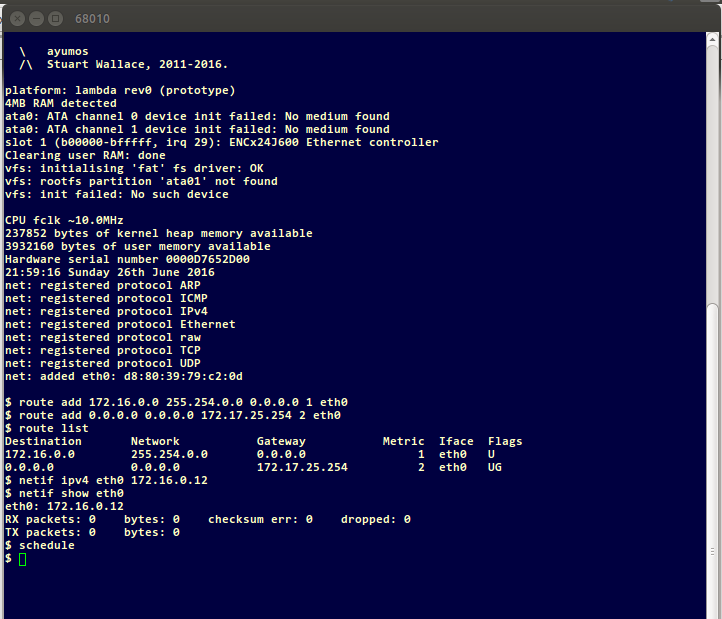
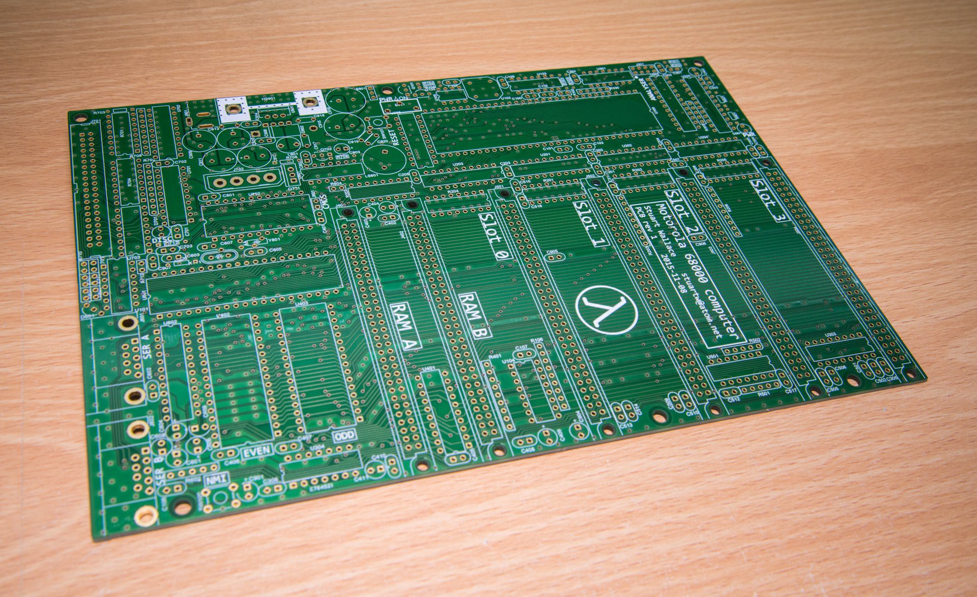
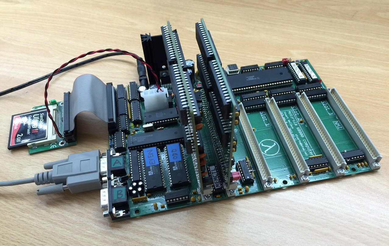
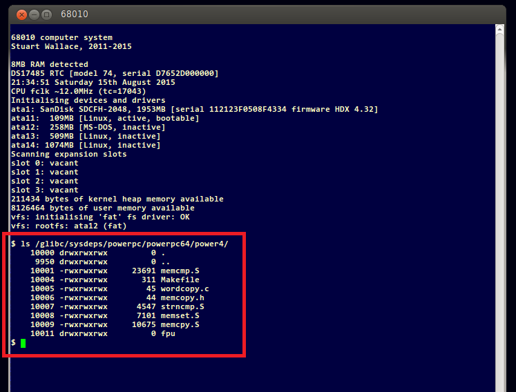
Motorola 68000 computer
A mc68k-based computer motherboard, some expansion cards, and a very basic multitasking OS, all built from scratch.
 Stuart
Become a Hackaday.io member
Already have an account? Log in.
Just one more thing
To make the experience fit your profile, pick a username and tell us what interests you.
Pick an awesome username
hackaday.io/
Your profile's URL: hackaday.io/username. Max 25 alphanumeric characters.
Pick a few interests
Projects that share your interests
People that share your interests
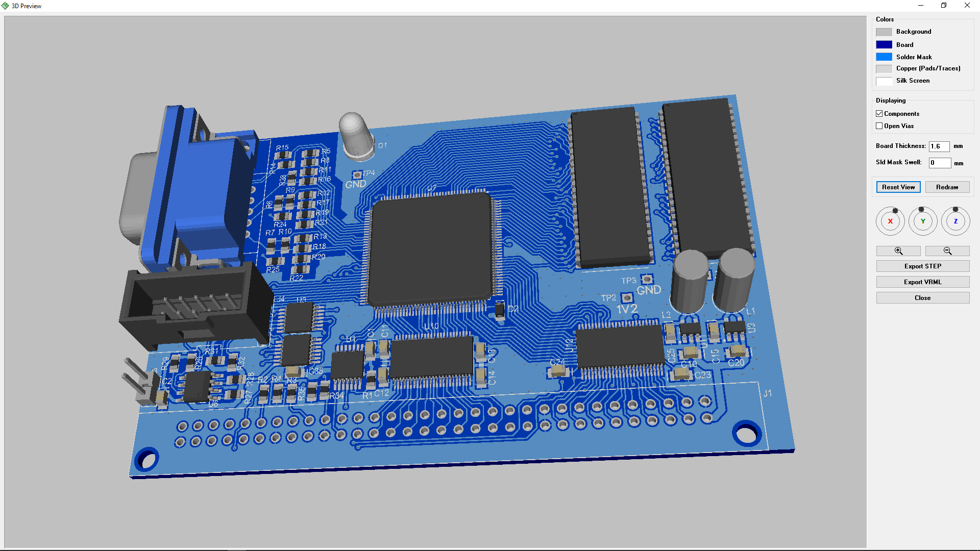
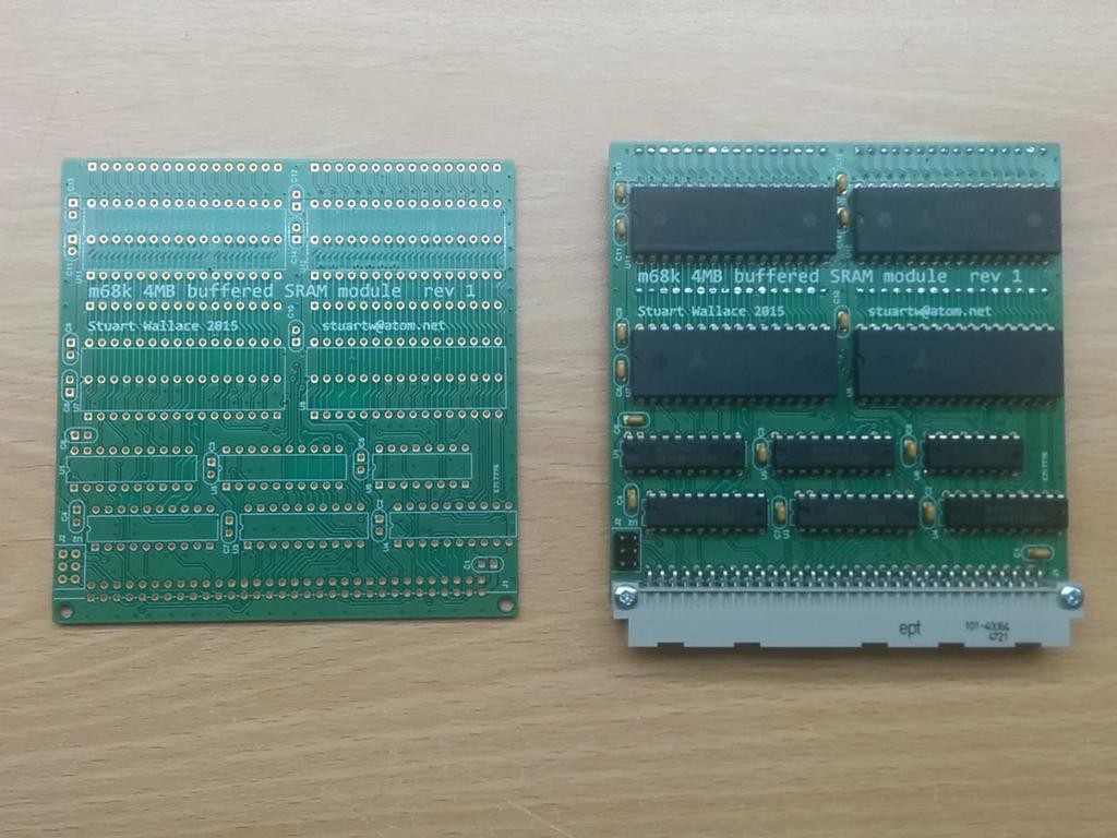
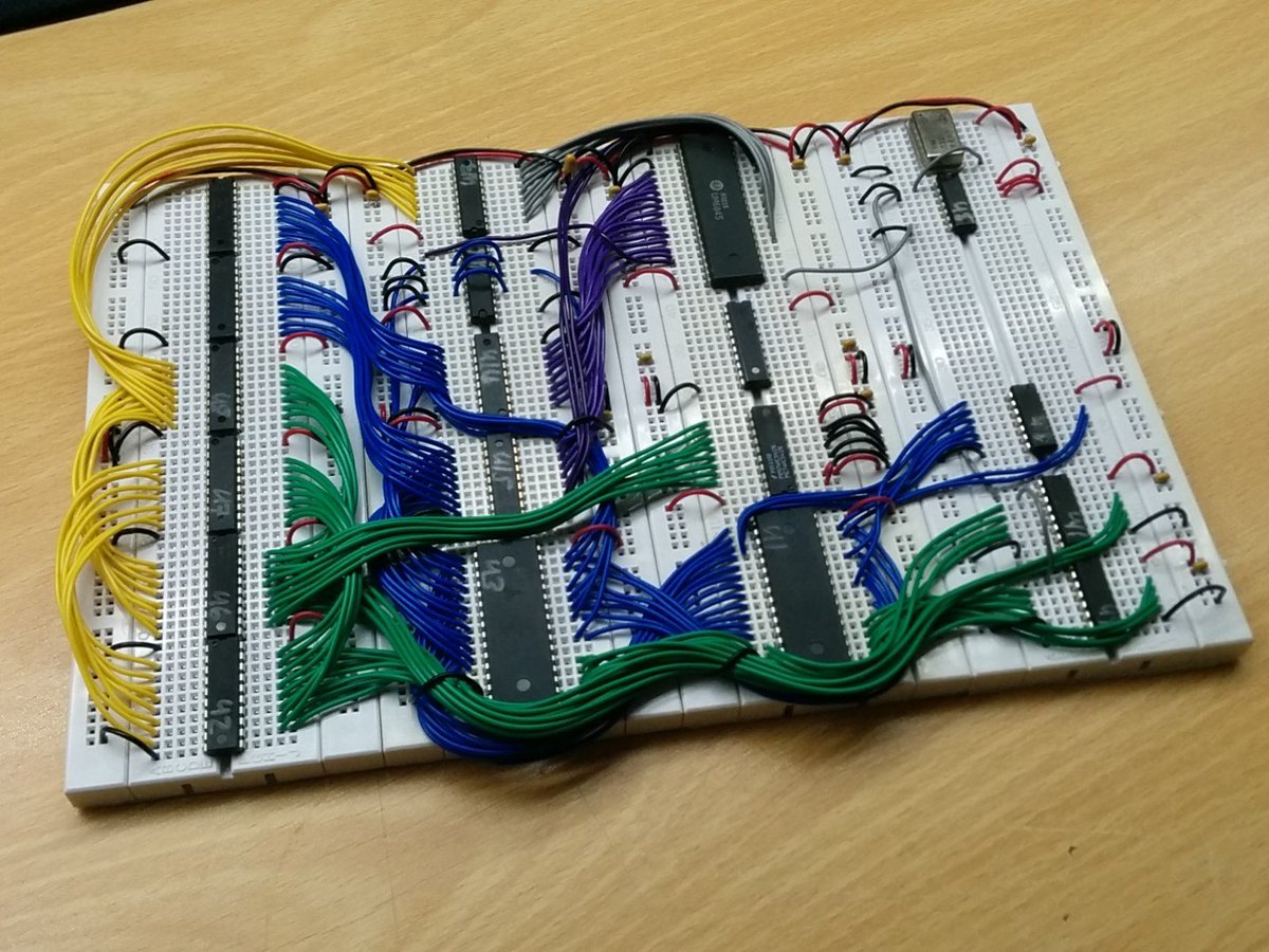 I became a bit demotivated when the time came to route the (gigantic) PCB. I have already routed one fairly gigantic PCB (the motherboard), and it can be a real time-sink. So: I ended up breaking a few of my own rules.
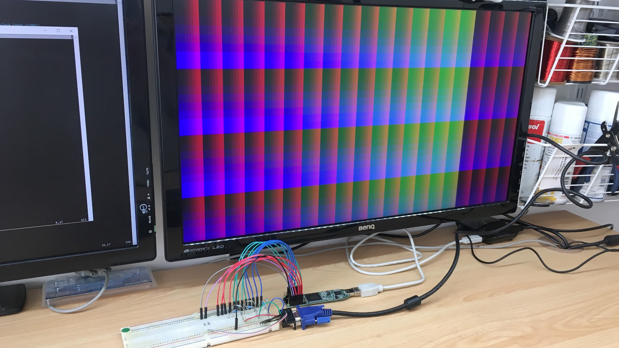


 Carson Herrington
 tomcircuit
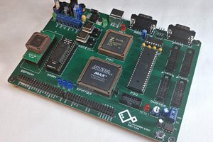
 Colin Maykish
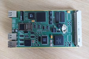
 Tom
Tom
for video have a look at this interesting proposed image format from the 90's it claims to offer true color performance with only 16 bits. https://r0k.us/graphics/png16Tech.html#fc16 who knows it could be fun implemented in hardware.