0%
0%
LiPo Charger + Boost
LiPo Charger with Load Sharing and Boost Converter
 Suleyman Hashi
Become a Hackaday.io member
Already have an account? Log in.
Just one more thing
To make the experience fit your profile, pick a username and tell us what interests you.
Pick an awesome username
hackaday.io/
Your profile's URL: hackaday.io/username. Max 25 alphanumeric characters.
Pick a few interests
Projects that share your interests
People that share your interests
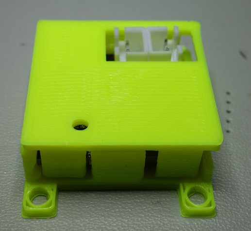
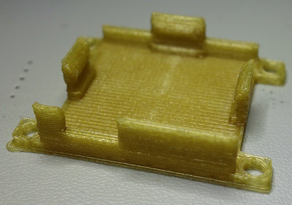
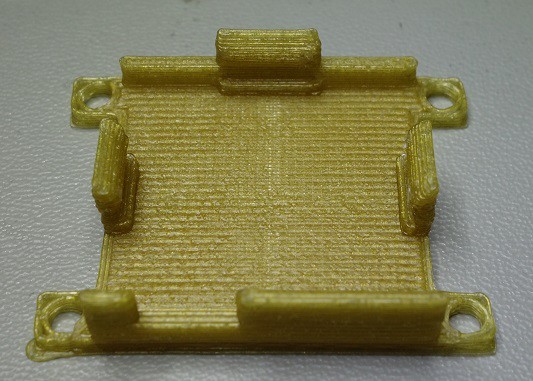
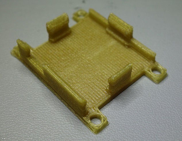
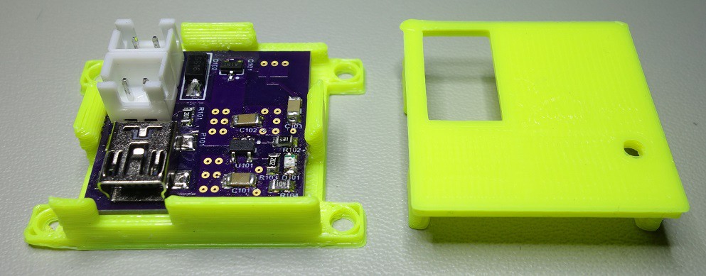 Another view, outlining the tabs on the top part.
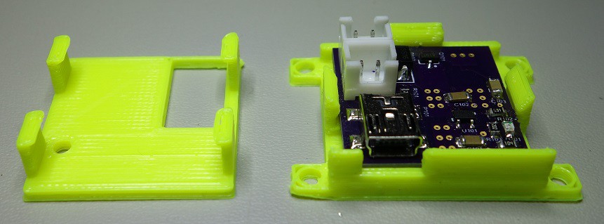 Below is when it parts clips into together.
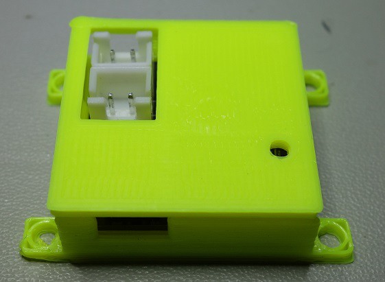
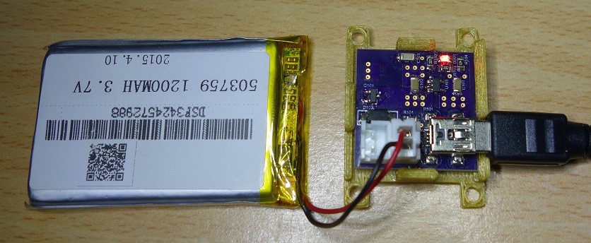
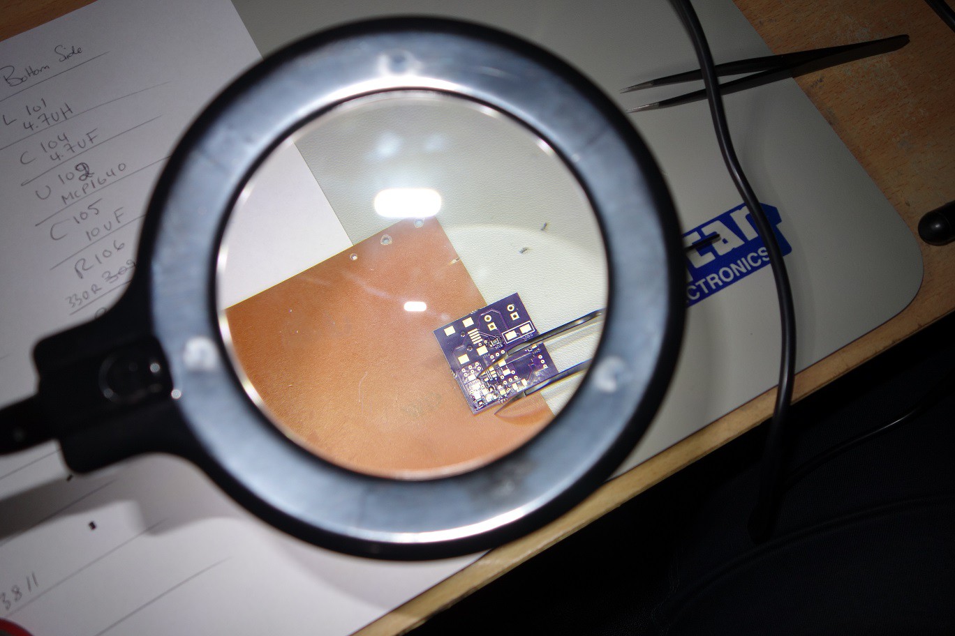
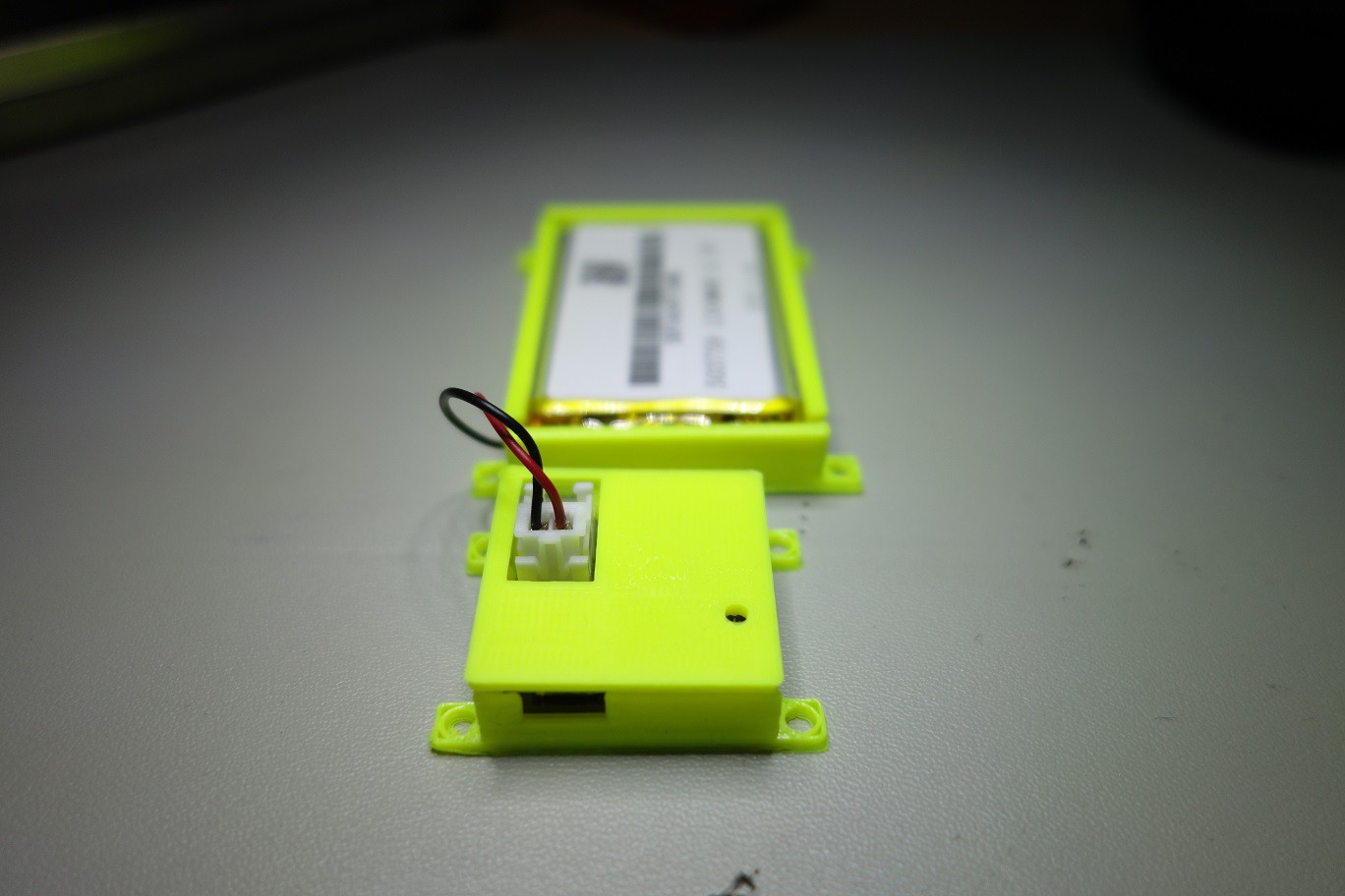 The red LED is only on when a battery is present and the battery is charging, otherwise its off.
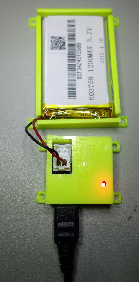 Test of confidence, by powering from my computer's USB port. I have been using a cheap mobile phone chargers from this.
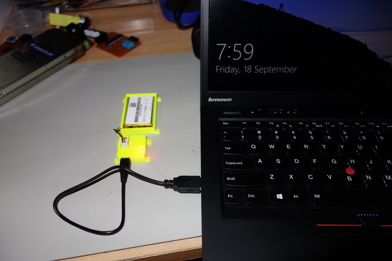
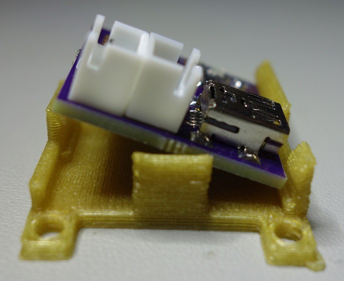
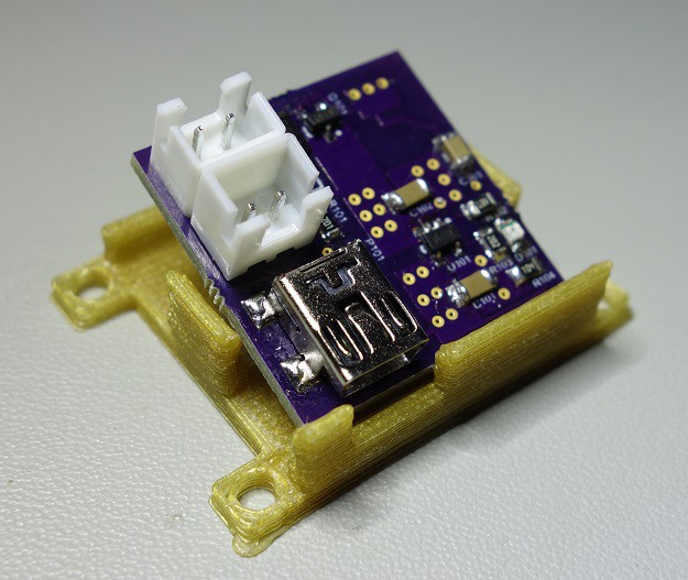
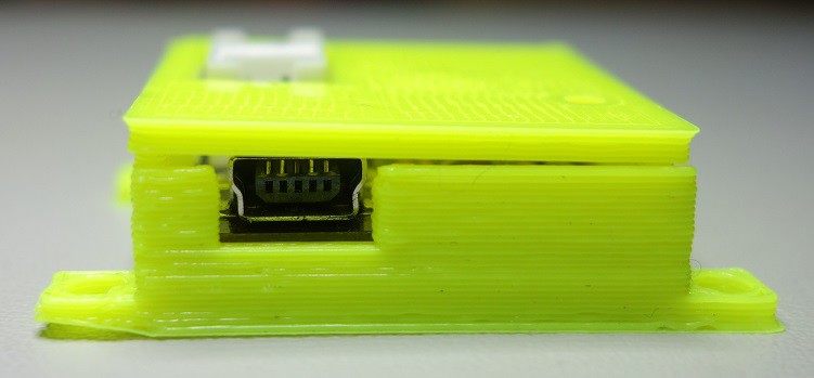
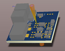
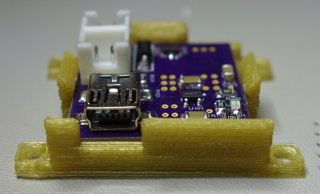 Notice that USB connector is too recessed and might require moving the connector more outwards.
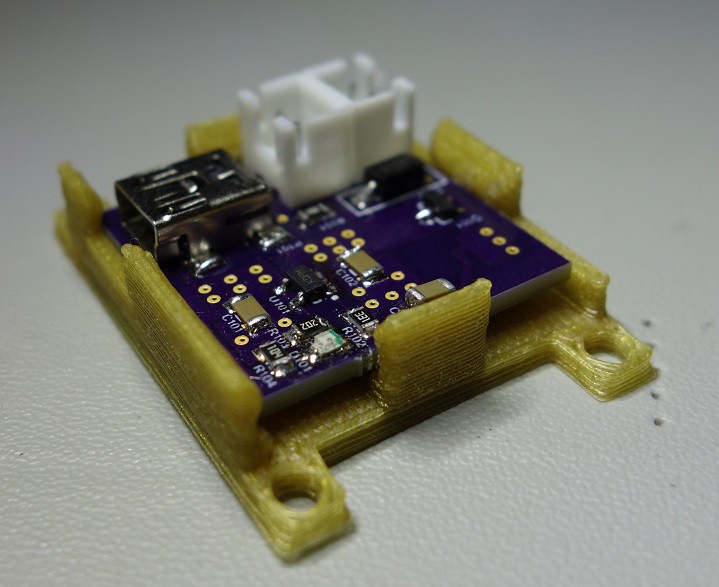
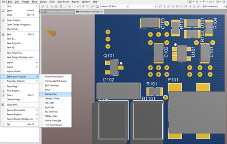

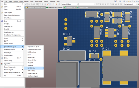
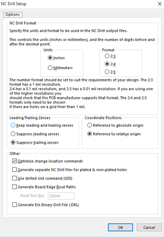
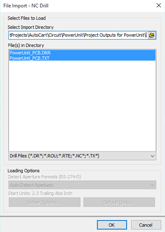
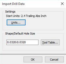
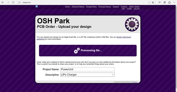
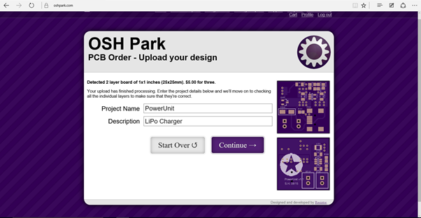
 The CAM file should be in view, however, there is no holes present. Therefore we need to generate the drill files.
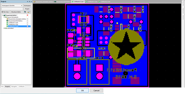
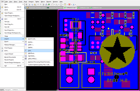
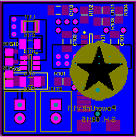


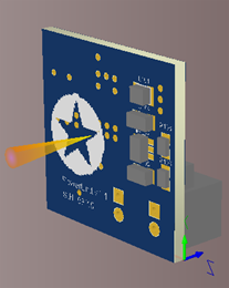
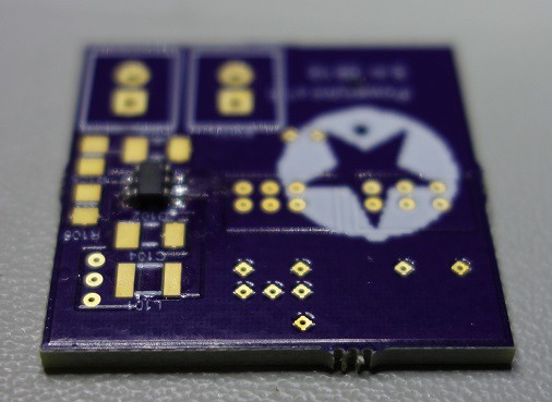
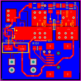 Top layer of my PCB, I have hid the top overlay.
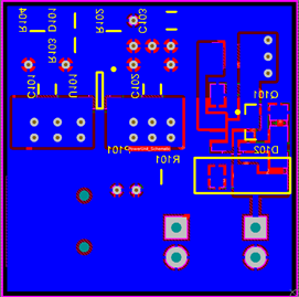
 I was informed by
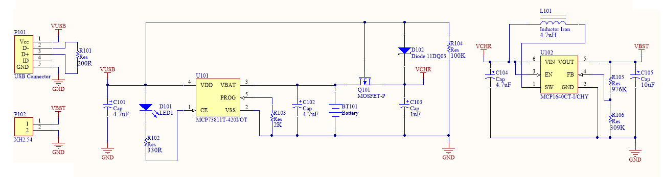

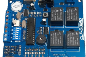
 Jefferson Bueno
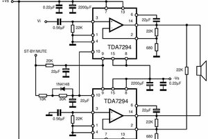

 Budi Prakosa a.k.a Iyok
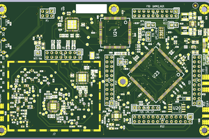
 Stanislav
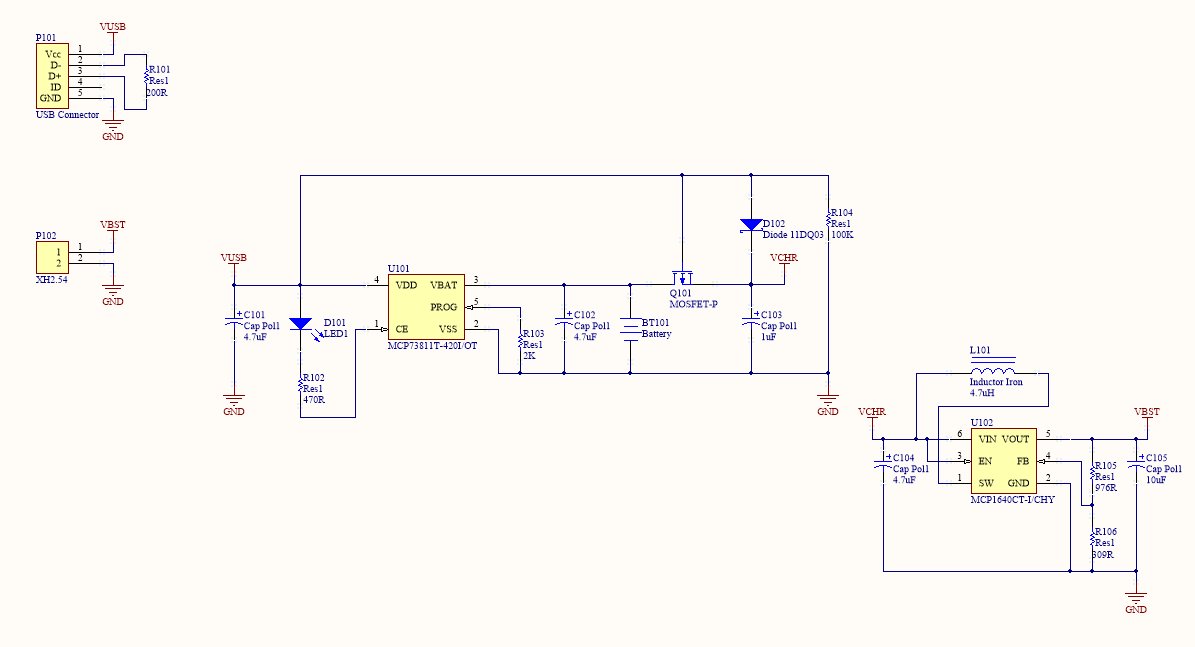
I would like to see the schematic