Close
0%
0%

Ionic Thruster Power Supply

HVDC power supply that provides +54kV, -54kV, and -73kV with minimal voltage ripple and moderate output current.

Similar projects worth following
Safety First: The voltage and current levels utilized within this project can harm or kill without physical contact. If you have not dealt with high voltage before, please find and read a high voltage safety manual before operating any of the circuits described in this project.

The power supply design is modular and allows for stacking parts of the system to produce higher voltages and currents. The overall system is a multistage SMPS topology that uses high efficiency multipliers to produce the higher voltages. The conversion chain is as follows:

220 VAC -> 390 VDC -> 1.95k VDC -> +54k, -54k, -73k VDC

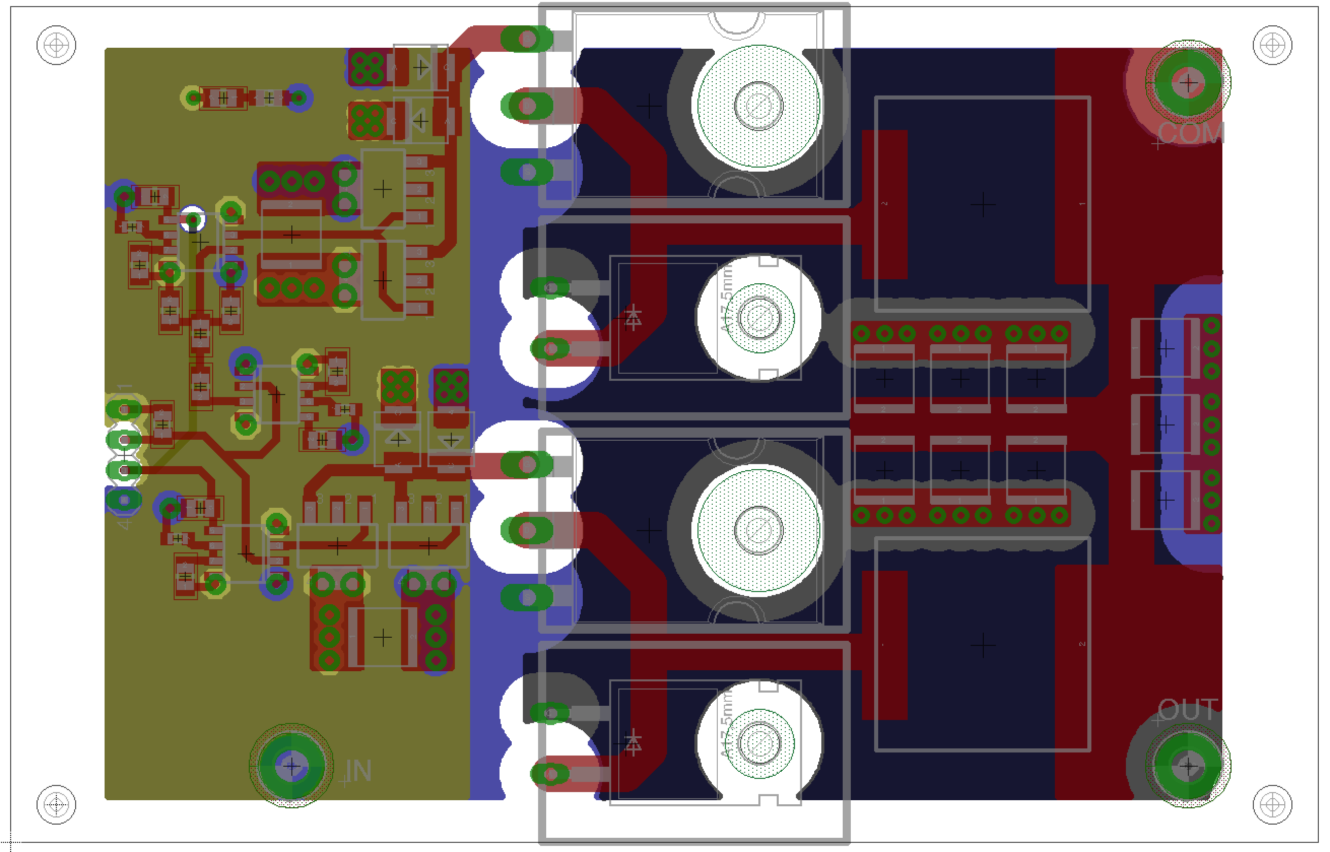
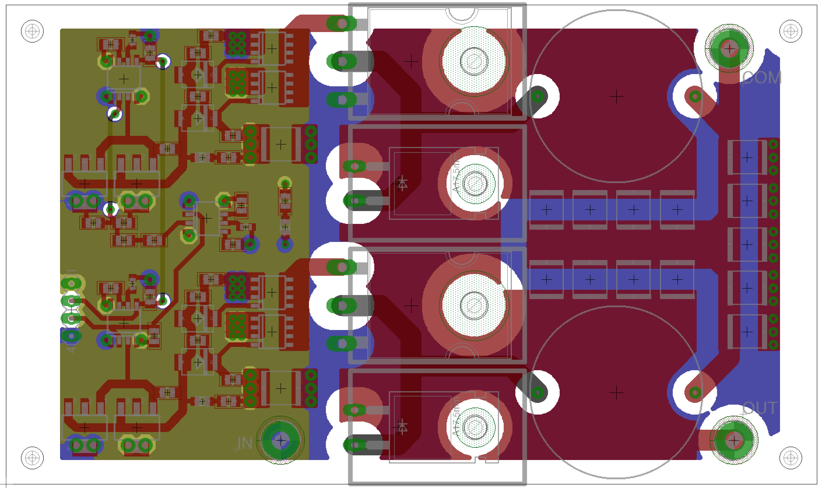
The power supply is comprised of four stages:

  • AC Mains to 390V DC converter
  • Current limited 390V DC to 1950V DC converter
  • HV Multiplier Driver
  • HV Multiplier

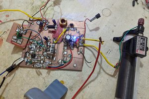
The HV multiplier and it's driver are the core of the project. Together they convert the 1950V DC to >50kV with an efficiency of >98%. This high efficiency is obtained by driving a tuned circuit at its resonant frequency with saturated switching. The use of resonant elements improves the multiplier efficiency by both reducing the amount of voltage sag between multiplier stages and by spreading the diode current across the full AC cycle. In traditional multipliers that only use capacitors for the AC-pass elements, the diode current takes the form of short, high-current pulses at the peaks of the AC voltage. The short current pulses result in a higher forward voltage in the diodes and increase the resistive losses in the circuit. Using resonant AC-pass elements smoothes the pulses and reduces the power losses in the diodes. An additional benefit to using resonant elements is that they have a near-zero impedance at their resonant frequency which further reduces the voltage sag between stages.

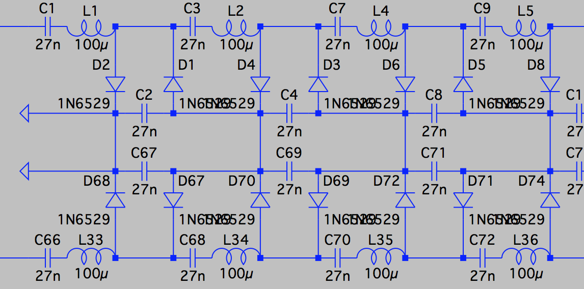
Using the values from the image above, here are some quick numbers:

  • Resonant Frequency: 96.91 kHz
  • Operating Frequency: 96.99 kHz
    • 0.1% deviation from ideal excitation frequency
    • constrained by 555 timer, component tolerance of 0.5%, and component availability
  • Element Impedances
    • Capacitor: 27 nF @ 96.99kHz = 0 - j60.81 Ohms
    • Inductor: 100 uH @ 96.99kHz = 0.560 + j60.91 Ohms (includes real resistance from winding)
    • Combined: 0.560 + j0.10 Ohm (note that the imaginary impedances cancel)
  • Efficiency Estimation
    • The inductor saturation current is 700 mA. This limits the maximum input current to 490 mArms.
    • With 28 stages this produces an output current of 8.75 mA. (Note: 28 * 1.95kV is roughly 56kV)
    • The driver output is a 1950 Vp-p square wave. This is equivalent to 975 Vrms.
      • The maximum input power is therefore 477.8 W, and since the circuit operates at resonance, the phase alignment between voltage and current results in a purely real power factor.
    • The total power loss is a combination of the diode losses and the pass-element losses.
      • Diode Forward Loss: 56 * 1 V @ 8.75 mA = 490 mW
      • Diode Reverse Loss: 56 * 50 uA @ 1.95 kV (50% duty cycle) = 2.73 W
      • Pass-Element Loss: 28 * 0.56 Ohms => 1.323 W
      • Combined Result: loss of 4.543 W
        • Output Power: 477.8 W - 4.543 W = 473.2 W (99 %)
        • Output Voltage: 473.2 W / 8.75 mA = 54.08 kV

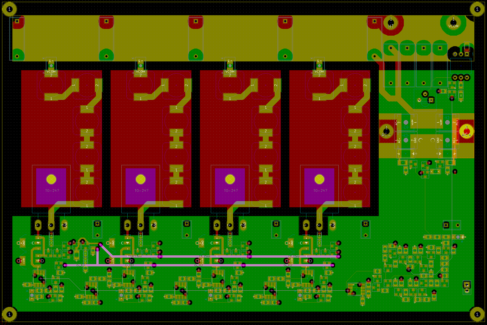
The final design calls for 4 drivers to provide phase shifted outputs. By using poly-phase input power and combining the multipliers in parallel the output ripple is reduced by a factor of 16 from 188 Vp-p to 12 Vp-p. The final design calls for 16 multipliers divided into positive and negative output groups to provide +54 kV @ 70 mA and -54 kV @ 70 mA. The combined maximum power output would be 7.5 kW.

For details about the application of the power supply, please see #Ionic Thruster.

PFC.zip

KiCad project files for 1kW PFC module (220 VAC)

Zip Archive - 86.80 kB - 11/26/2016 at 04:07

Download

controller.brd

clock generator and fault detector for driver boards

brd - 125.23 kB - 01/20/2016 at 22:58

Download

driver.brd

2kV square wave generator

brd - 110.81 kB - 01/20/2016 at 22:58

Download

isolator.brd

AC pass and DC blocking circuit for exciter input

brd - 75.39 kB - 01/20/2016 at 22:34

Download

exciter.brd

10 stage HV multiplier

brd - 66.35 kB - 01/20/2016 at 22:34

Download

View all 6 files

  • 28 × TYS5040101M-10 Inductor: 700mA, 100uH, 2220 SMD
  • 56 × 2220GC273KAT1A Capacitor: 2kV, 27nF, 2220 SMD
  • 56 × CD214A-R12000 Diode: 2kV, 1A, DO-214AC SMD
  • 2 × STW11NM80 MOSFET: 800V, 11A

  • PFC Revision

    Robert Rouquette11/26/2016 at 04:24 0 comments

    Finally getting back to this project after quite an absence. Currently working on getting the design of the 2kV power chain completed. Also taking the time to learn KiCad. A screen shot of the PFC board is included below. New PFC design boasts 400V @ 2.5A output with 220VAC input. Input EMI filter and output 8800uF capacitor bank are off-board. The switching frequency is 100kHz, and the circuit utilizes polyphase switching to minimize HF ripple and noise. Loose output voltage regulation is achieved through cycle-skipping, which preserves both the high power factor and the high efficiency of the PFC: 95% @ 1kW, 91% @ 250W. The design does not require discrete heat-sinks and uses steady airflow to maintain optimal temperature.

    The 15V power plane is hidden in the image, but it has the same footprint as the ground plane. (green L-shaped layer)

  • Earlier Work

    Robert Rouquette01/26/2016 at 16:08 0 comments

    I found some photos of previous multiplier prototypes I built last year. The Image on the left is the very first set which were a 20-stage negative multiplier and a 20-stage positive multiplier. They produced several microamps at +/- 26kV and used a electronic ballast as the input source. The image on the right is the first resonant multiplier board. The board includes a resistor voltage divider and was designed to be oil immersed and produced a few hundred microamps at +/- 40kV using the same ballast as input.

  • PFC Module Revision

    Robert Rouquette01/26/2016 at 01:50 0 comments

    Replaced the unshielded inductors with shielded ones. Increased the switching frequency, which allows for smaller filter capacitance and a better power factor under light load. Power factor and efficiency at max load are unchanged. Layer order for high voltage planes was modified to reduce parasitic capacitance on the flyback traces and voltage stress on the board dielectric.

  • System Block Diagram

    Robert Rouquette01/25/2016 at 04:08 0 comments

    Here's how all of the various boards work together. The multiple conversion stages are required to provide a high end-to-end efficiency as well as support throttle control and safety interlocks.

  • PFC Module

    Robert Rouquette01/25/2016 at 03:12 0 comments

    Design of the PFC module for the AC-to-DC converter is nearly complete. Each module provides a 1kW output at 340V with a power factor of 0.99 and an output efficiency of 96% with an input voltage of 240 VAC. These modules can be combined in parallel to provide higher output power. Each of these boards contains two non-isolated buck-boost converters that can operate over an input range of 120 - 410 VDC or 90 -270 VAC with an external rectifier and EMI filter. The two converters are operate out-of-phase with each other to minimize EMI and the capacitor ripple currents. Each of these boards are controlled from a central board that provides the reference clock and feedback for limiting the output voltage when the output is not sufficiently loaded.

    I plan to have the board and BOM finalized by the end of the week. I hope to build and test a single PFC module near the end of next month.

View all 5 project logs

Enjoy this project?

Share

Discussions

DeepSOIC wrote 01/21/2016 at 09:26 point

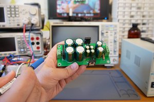
Don't forget to add bleeder resistors!

  Are you sure? yes | no

Robert Rouquette wrote 01/21/2016 at 13:51 point

Good catch.  I do plan to add voltage dividers on the outputs to provide feedback for monitoring purposes, and I have found that the 1G resistance in the dividers is sufficient.  The diodes also have a few micro amps of leakage that drain the circuit by about 100 V/s in each stage.  From past measurements, it typically self discharges to safe levels in about a minute without bleeder resistors.

  Are you sure? yes | no

Similar Projects

Does this project spark your interest?

Become a member to follow this project and never miss any updates