Close
0%
0%

muCPU: an 8-bit MCU

An 8-bit load-store CPU with 2 pipeline stages, designed in Logisim and implemented in VHDL + assembler written in Python

Similar projects worth following
A while ago I started building a 32 bit MIPS processor in Logisim. A while after that project was underway, I got an FPGA development board (miniSpartan6+). Although I probably could squeeze the 32 bit version on the FPGA, I am new to the world of programmable logic (vhdl, verilog, etc.) so I decided to build a very simple, very small (hopefully) CPU core. I've included the instruction set in a google doc in the links section, as well as a link to the github.

(I will be updating this at https://github.com/reed-foster/uCPUvhdl/wiki and eventually will remove this section)

Designing a CPU:

In this section, I will describe how the muCPU was designed and how it works. Any blocks of text in italics is information to explain why I made a certain decision; it does not need to be read to understand how the muCPU works.

Step One: Instruction Set

When designing a CPU, the first thing to consider is what features/capabilities you want it to support. There are two main design philosophies when it comes to designing instructions for an architecture. Originally, when computers first emerged, memory was very expensive, so data and instruction widths were kept to a minimum in order to reduce cost. In addition, processors supported a wide variety of simple to complex instructions; they supported memory addressing for arithmetic operations, and some instructions executed multiple steps. Programmers used a small amount of complex instructions to minimize memory usage. However, with technological advancements and shrinking transistor sizes, manufacturers could fit more and more transistors onto integrated circuits, improving the storage capacity and processing power of computers. With an increase in storage capacity, programmers didn't have to worry as much about how many bytes their code took up; instead, they could focus on the speed of their code. With this increase of memory came the second design philosophy known as RISC, for Reduced Instruction Set Computing (while the previously mentioned design philosophy came to be known as CISC, or Complex Instruction Set Computing) . RISC processors are designed based on the idea of executing many very simple instructions very quickly, rather than a few complex instructions that each take a while to execute. Since CISC style processors are inherently more complicated to design, often times with multiple instruction bit widths and very complicated decoding circuitry, I decided to base the muCPU design off of a very simple (in some aspects) RISC style instruction set: MIPS. The MIPS Instruction Set consists of three types of operations: r-type, i-type, and j-type. As one might suspect, the "r" in r-type is for register, while the "i" and "j" in i-type and j-type are for immediate and jump.

MIPS is a load-store architecture (meaning that memory is only accessed through load and store operations; arithmetic is done with a register file, a small bank of very fast memory) implemented with a pipeline, in fact, its name used to stand for Microprocessor without Interlocked Pipeline Stages. This basically means that each section of the pipeline takes one clock cycle to execute. MIPS uses a classic five-stage RISC pipeline consisting of the following stages: Instruction Fetch, Instruction Decode (and usually operand fetch), Execute, Memory Access, and Write Back. One of the problems with pipelining is that it introduces situations known as hazards. Hazards include structural, data, and branch hazards. Structural hazards are usually eliminated fairly easily; insert another adder here or there and usually all structural hazards are eliminated. Sometimes more complicated methods (such as register renaming) are required. Data hazards can occur when an instruction operates on data that has not yet been written back to the register file. Here's an example:

lb r2, 126(r5) ;load byte located in memory location (126 + contents of r5) into r2
add r2, r3, r4 ;add r3 and r4, storing the result in r2

The first instruction loads a byte from memory into r2, however, it takes 5 clock cycles for the instruction to be completed, so the second instruction will use an old value in r2, which is not what the programmer expects. One of the methods to negate this hazard is forwarding, a strategy that I used in my 32 bit MIPS CPU. In my implementation for that project, I save a small list of values and their corresponding register addresses that they are intended for. This list is located in the...

Read more »

spi.circ

SPI master and graphics coproccesor

circ - 25.06 kB - 04/18/2016 at 04:24

Download

muCPU[rev1].circ

Processor .circ file; requires installation of Logisim to run.

circ - 49.58 kB - 03/28/2016 at 00:11

Download

count.masm

Code that counts up to the number specified (at address 0x80) by the increment specified (at address 0x81). The updated value is written to address 0x82 every loop. Right click on RAM, choose load image, and then select this file.

masm - 65.00 bytes - 03/28/2016 at 00:10

Download

loadaddstore.masm

This code loads two values (at 0x80 and 0x81) into registers, adds them, and stores the result (in 0x82). Right click on RAM, choose load image, and then select this file.

masm - 44.00 bytes - 03/28/2016 at 00:10

Download

  • Drawing Bitmaps with Python

    Reed Foster05/29/2016 at 21:27 0 comments

    As soon as I discovered that I would have to run a script to convert .xbm files to an array that would be usable by SSD1306, I decided that I would write a simple python application to import .xbm files, draw new ones, and export the display data to an array with VHDL syntax. It took a while to get the GUI to work how I wanted, but eventually the app worked:

    Read more »

  • When In Doubt, Software!

    Reed Foster05/27/2016 at 03:38 0 comments

    With an almost complete loss of data between the SPI controller and the SSD1306, I decided that I should use just the processor core because I know that at least the processor core runs how it is supposed to (how the simulation runs) on the FPGA itself.

    Read more »

  • Potential Signs of Life

    Reed Foster05/14/2016 at 23:48 0 comments

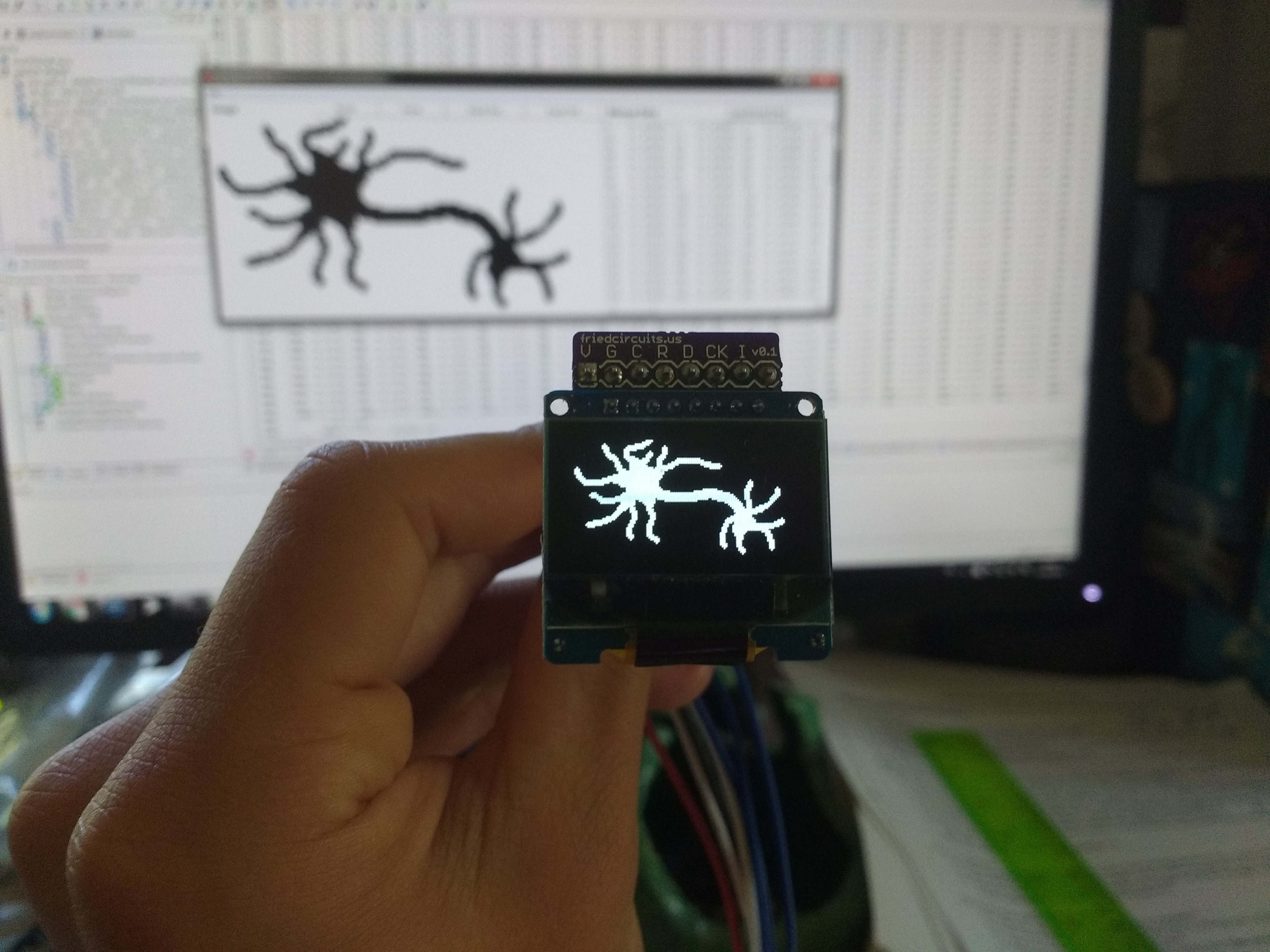
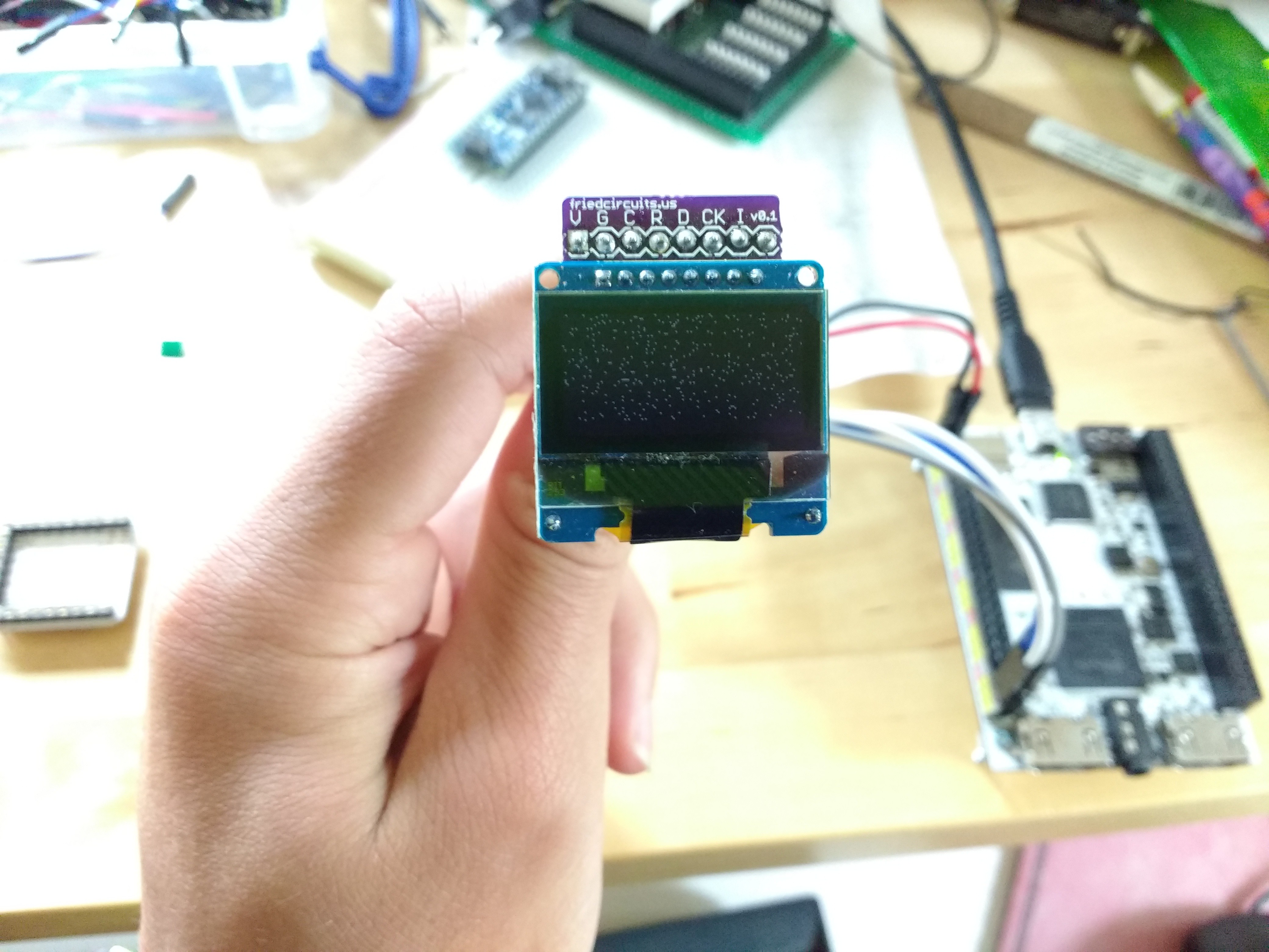
    I wrote some vhdl to connect the core module to my spi module that I created, as well as some assembly code. Looking at the simulation waveform, the display should theoretically display a blank screen, but that was not the case. The clock and data are slow enough according to the ssd1306 spec sheet, but I'll try a slower clock later (the whole spi controller runs off of the divided clock, so slowing the sclk will introduce problems with the fifo which will require some redesign, otherwise I would have already done it). Even though it is far from working, it's still exciting to see pixels light up on the display. As usual, commentless :( vhdl code is up on github.

    (side note: I have tested the display with an arduino, and it does work).

    Picture of the display

    SPI waveform

  • Lots of Updates

    Reed Foster05/08/2016 at 20:46 0 comments

    I've let some of the work I finished pile up, so here are several updates:

    I redesigned the memory, which now uses a 16 bit address, and provides 4KiB of ROM, 4KiB of RAM, and 4B of I/O (maybe need some more). The upper byte of the address is determined by the page address register (r7). The lower byte is the same as the old method, 8 bit immediate plus the base address register specified in the opcode. This is (sometimes) annoying because it takes two instructions to access a location in memory. Most of the time, however, there is only one instruction to set r7, and each memory access requires only one instruction. This occurs when the data being accessed is somewhat densely packed in memory. When the data is spread out, then it takes about 2 instructions on average to access each byte.

    I also decided to scrap the receive portion of the spi controller, and finished up the send portion.

    Read more »

  • VHDL FIFO

    Reed Foster05/04/2016 at 00:15 3 comments

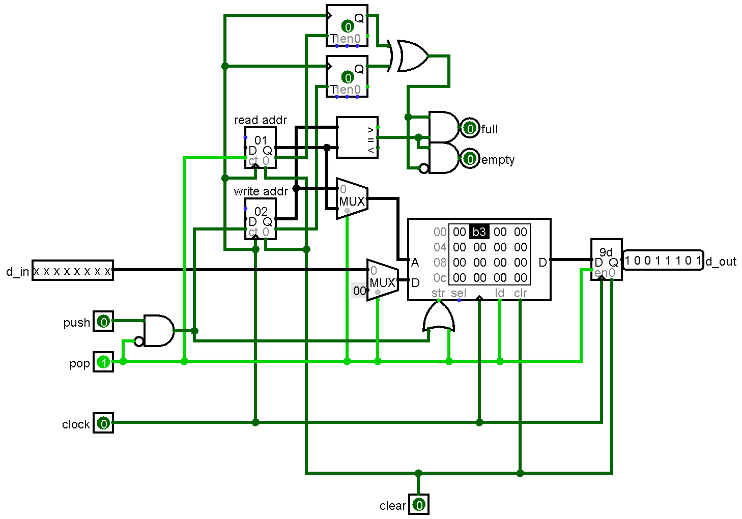
    Slowly, but surely, the VHDL code for the controller is coming along; I've just finished a structural architecture for a FIFO queue (first in first out). In a FIFO, data is "enqueued" (pushed in a stack) and "dequeued" (popped in a stack). However, the cool thing about queues (and stacks, for that matter) is that only a value must be supplied; the stack handles addressing. Below is a sample of enqueueing and dequeueing using a FIFO queue:

    Read more »

  • Improved SPI I/O in Logisim

    Reed Foster05/02/2016 at 00:13 0 comments

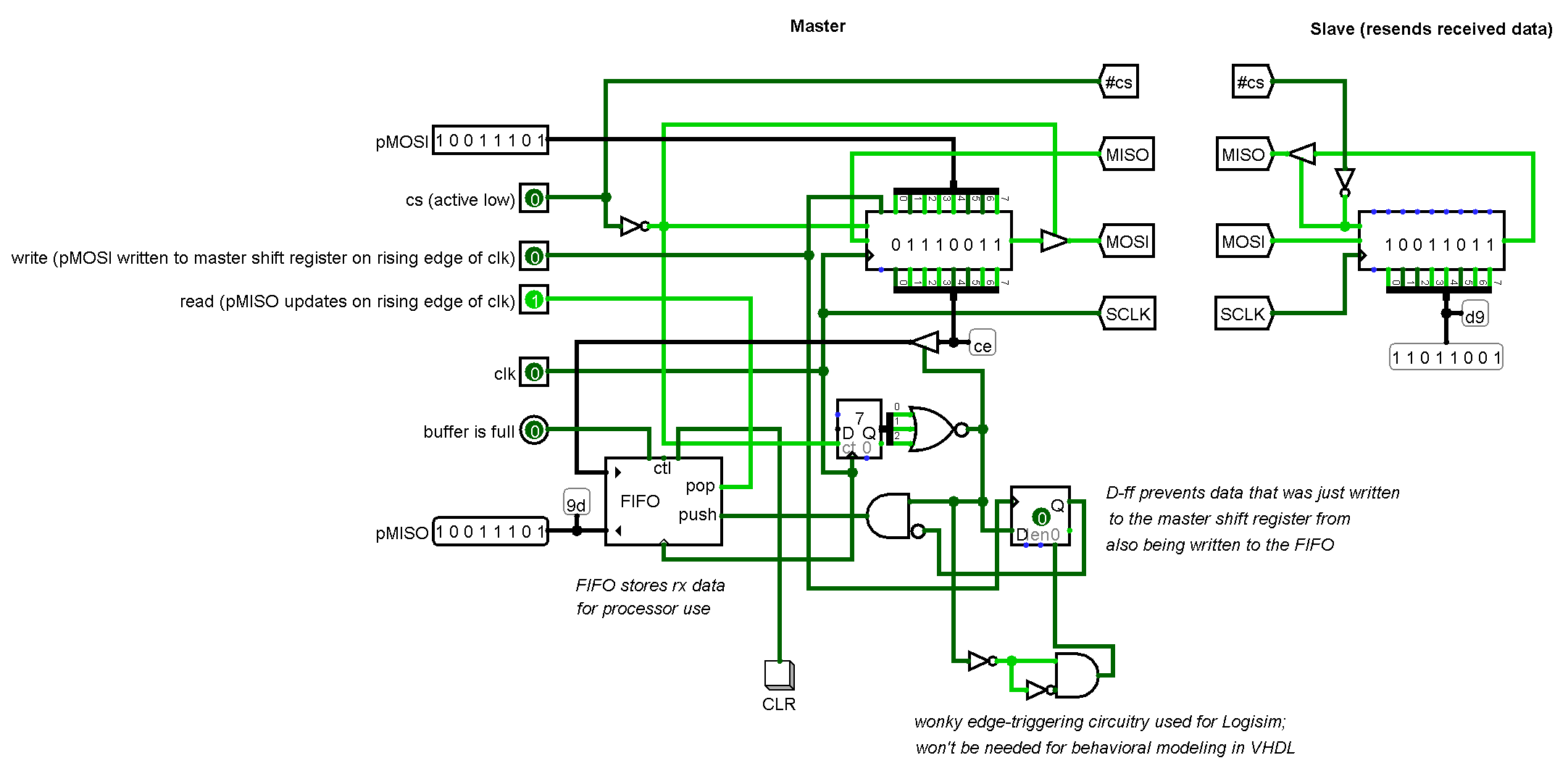
    This controller adds more functionality that the other lacked. The operation of the controller itself is almost entirely standalone and only requires an input of a clock signal and a steady address signal during operation. I added a FIFO to the input as well so that the data in the shift register is not overwritten when the write input pin is asserted. In addition, a D-FF is set whenever the write pin is asserted, and the flip-flop is only reset when the master has sent a byte and the slave is no longer sending data (might need changing depending on operation of slaves). The output of the D-FF is the cs signal, which is inverted for the ~cs line to the slave. Currently there are only two slaves; one sends the byte it receives back to the master, and the other sends a pseudorandom byte to the master. Here's the .circ file on Github.

    Read more »

  • SPI I/O in Logisim

    Reed Foster04/28/2016 at 04:42 1 comment

    Just finished a design for the SPI controller in Logisim. The slave doesn't really do anything; it shifts out what was shifted in, so when I run the clock for a while, the FIFO fills up with 2 different byte values (master initialized to one value, slave to another). Both the read and write functions are synchronous; the master's shift register only loads from the parallel port when the clock rises and write is high. Similarly, the FIFO only pops the value at the read address when the clock rises and read is high. Currently, with the limited functionality of Logisim block RAM, the FIFO cannot be written to at the same time as it is being read from; this will change for the implementation in VHDL. SPI circuitry below:

    FIFO stack (with less documentation of circuitry):

  • SPI I/O

    Reed Foster04/28/2016 at 00:49 0 comments

    I've decided to do away with the complicated video controller setup that I was starting to design. Instead of building what was going to effectively be a co-processor (with its own instruction set, memory, execution hardware...), I decided that I would leave it up to the processor to write the required bytes of data to the SPI controller. I will design a more generic SPI controller that supports input as well as output and 16 slaves (maybe more). I might still keep an external memory to store the initialization sequence for the display. For now, it's just an idea, code and schematics to come later...

  • Graphics Controller

    Reed Foster04/18/2016 at 04:21 0 comments

    To provide data for the SPI master, a graphics controller is needed (otherwise the processor is bogged down with simple loads and stores). I built a circuit in Logisim that seems to do the job. I've uploaded the .circ file to github, and included a screenshot below:

    Read more »

  • MOAR I/O! (SPI)

    Reed Foster04/18/2016 at 00:05 0 comments

    I have a couple oled displays lying around, and I figured that the display wouldn't be too complicated to interface to (riiiight). Anyway, the OLED controller (SSD1306) is configured to communicate with SPI, so to talk to it, I need an SPI master entity that takes an 8-bit parallel value and loads it (serially) into the OLED. I also wrote an arduino sketch based off of Adafruit's library for the SSD1306. By writing this sketch, it is easier for me to understand what exactly needs to happen to a) initialize the display and b) write data to it to display pixels (and hopefully characters and words eventually). The vhdl code I've written may not be the most efficient code, but it appears to work. I've uploaded the vhdl file for the SPI master (as well as its testbench) to github, and below is an (edited) image of the iSim waveform output:

    Read more »

View all 14 project logs

Enjoy this project?

Share

Discussions

Yann Guidon / YGDES wrote 09/18/2016 at 22:25 point

Very nice description of the architecture :-)

  Are you sure? yes | no

Similar Projects

Does this project spark your interest?

Become a member to follow this project and never miss any updates