PARTS
It will consist of the following parts:
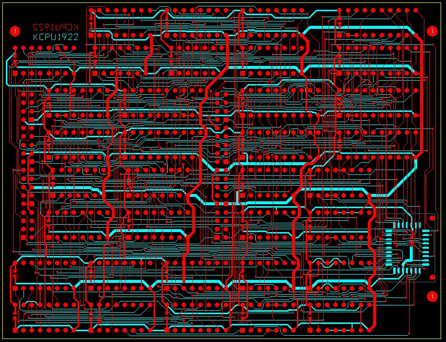
- processor in the spirit of the #1 Square Inch TTL CPU
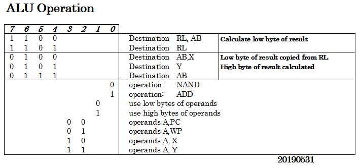
- a simple ALU (described here)
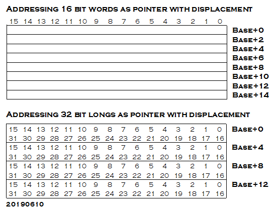
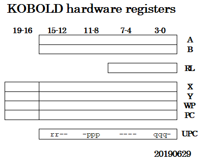
- some address registers (described here)
- at least 256 KByte RAM
- flash-ROM for booting
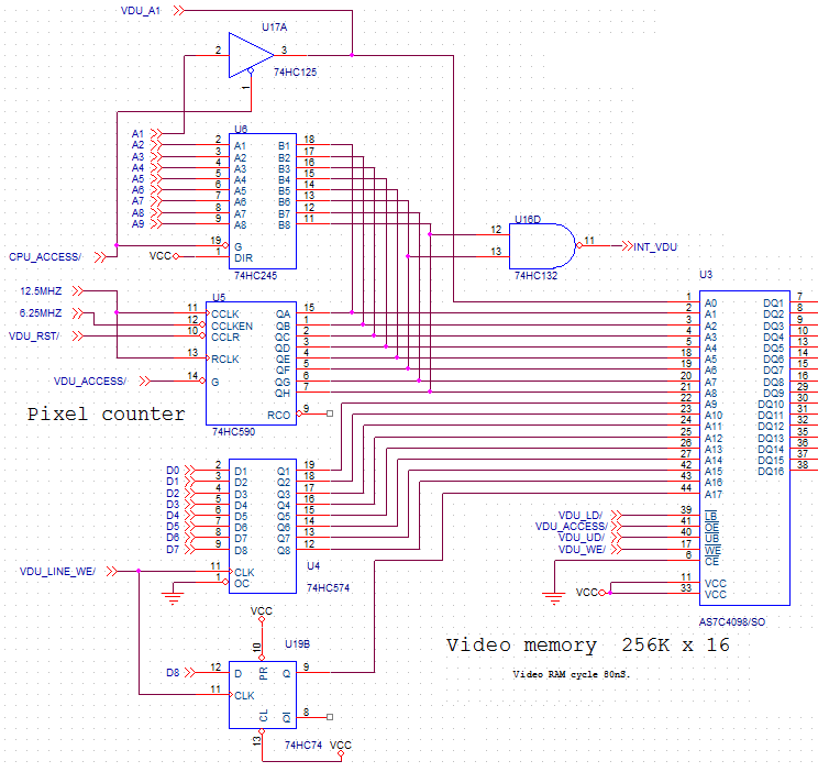
- VGA video
- PS/2 keyboard input
- user-accessible I/O pins (footprint of Arduino shield)
- a sound system
- serial flash (16 or 32 MByte) for storing all your programs.
VIDEO MODES
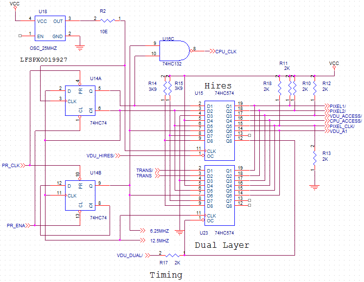
- Mode 1, 640 x 480 bitmapped pixels, color. Gives at least 80 x 25 text capability.
- Mode 2, 320 x 240 (or 320 x 480) bitmapped pixels, color, dual layer.
Mode 1 is described in this log.
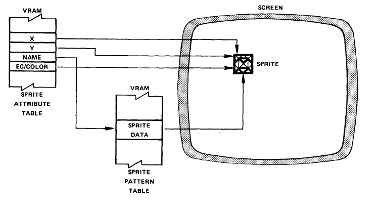
Mode 2 has two layers, (foreground and background), enabling sprites (see this log).
Video mode 1 or 2 can be selected per line.
Support for fast vertical scrolling.
number of colors: 128
At this moment, the idea is that the CPU and the video part will operate quite independent. The CPU might even be a separate pcb that is placed on top of a "motherboard", that has the memory, video and other I/O.
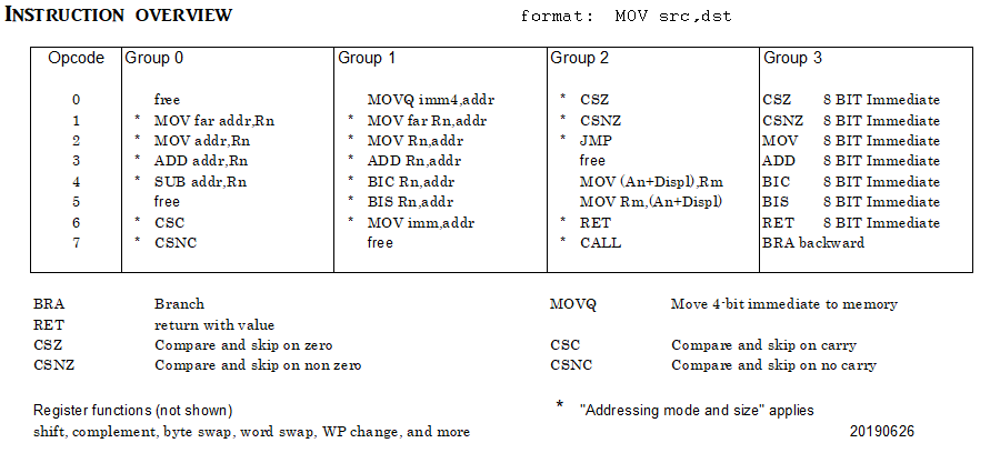
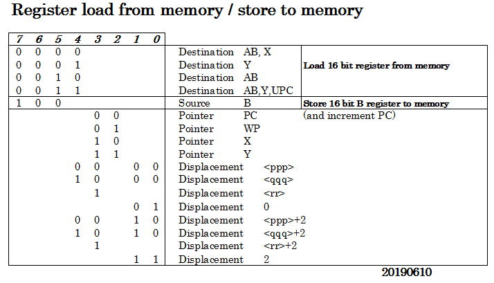
INSTRUCTION SET
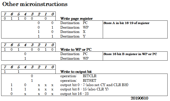
The instructions will be implemented in microcode (defined HERE). There will be two main instruction sets:
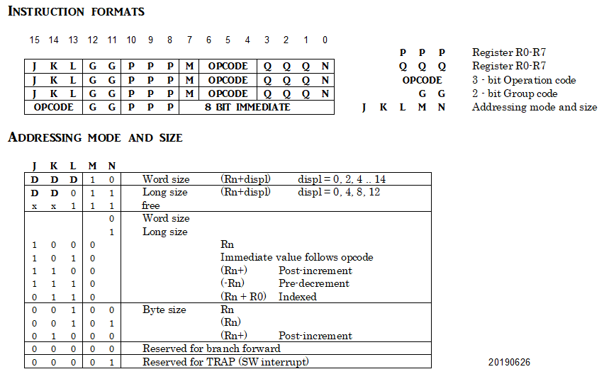
- The native 16-bit Kobold instruction set has highest execution speed and very good code density. The instructions are similar to 68000 and PDP-11 instructions and can handle 8, 16 or 32 bit data size. The instructions can access 1 MByte of memory.
- The K11 instruction set will be binary compatible with the PDP-11 instructions. It is kept in mind, but will only be given full attention after most other goals are reached. It might become a separate project.
The microcode can be easily reprogrammed with a Raspberry Pi as programmer (just as with the 1 Square Inch TTL CPU ). The microcode Flash is large enough to accomodate a lot of microcode.
The CPU will probably be around 35 TTL parts and a microprogram Flash.
PROGRAMMING
A Raspberry Pi can be connected, that can read or write files from or to the serial flash of the Kobold.
When enough supporting software is in place, the programs for Kobold can be developed on the device itself, perhaps first in BASIC and later in C.
PLAN
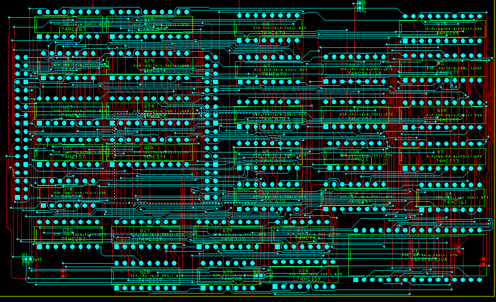
- design the CPU
- pcb design of CPU with thru-hole components
- design the motherboard
- pcb design of motherboard
- some simulations
- order boards, and assembly
- hw fault finding
- build an assembler and programming software
- pcb design of a small Kobold CPU in SMD version
- build or adapt a C compiler
- make system software. Might adapt an OS.
This is a work in progress, the logs will show the design steps....


 Ed S
Ed S
 Pavel
Pavel
Flipping through my notes of more than 2 years ago, today I discovered that we *did* briefly consider using a 16-bit register file with tri-state outputs: the 74172 !! But then we found a remark about its extinction on http://www.6502.org/users/dieter/tarch/tarch_2.htm and we moved in a different direction. It never occurred to me there might be later 74 numbers with a (somewhat) similar function. Cool find! While I now like that the resulting Gigatron has no state hidden in the TTL chips (everything can be probed), this is a bit subjective and the Kobold looks pretty impressive as well. Looking forward to its operation.