-
Mary Ann (Part 1) Breadboarded
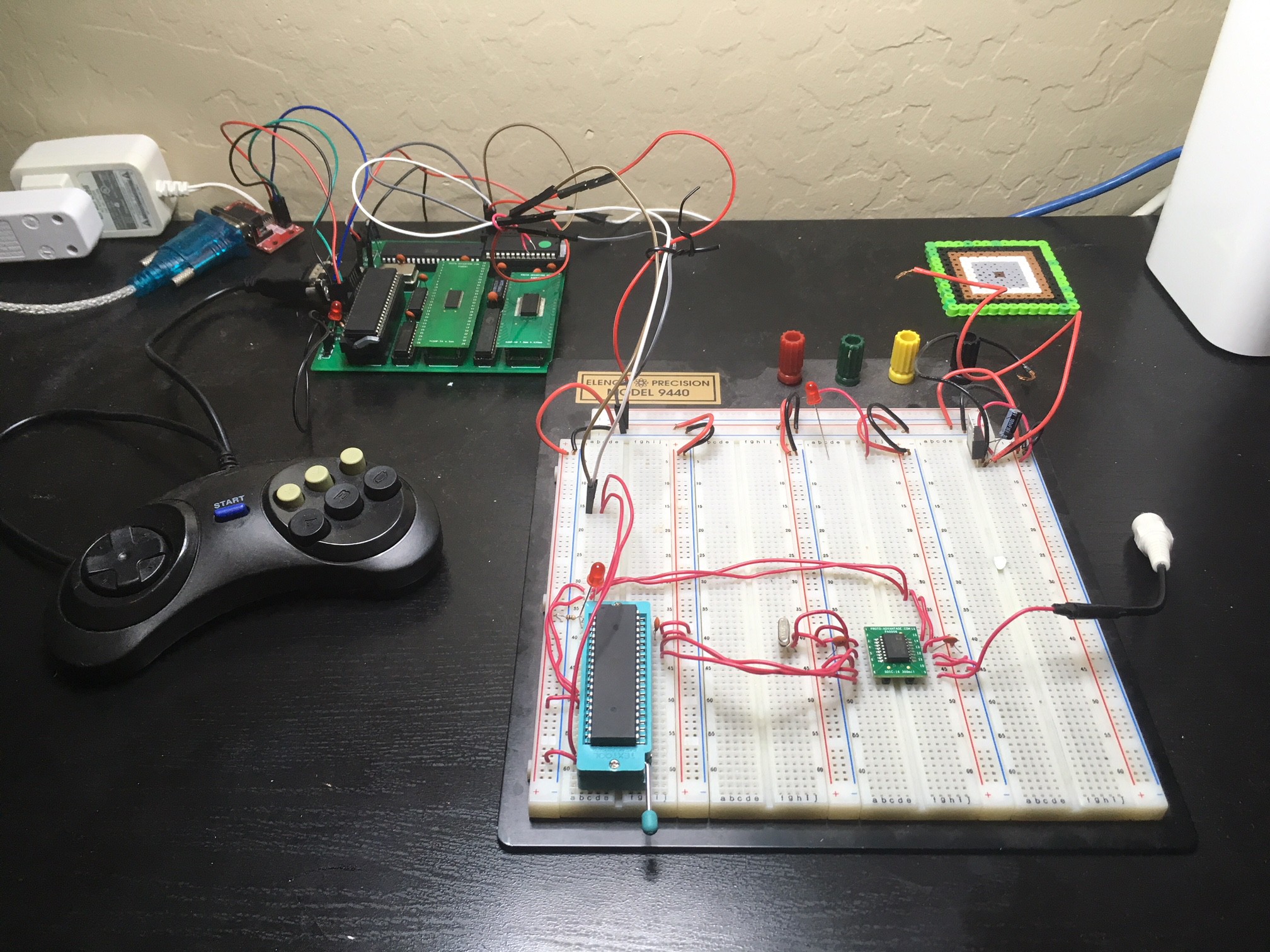
06/05/2018 at 07:06 • 0 commentsThe AD724 arrived today - so after the family went to bed I stayed up breadboarding everything. I think it's all ready to go and I'll start writing the code tomorrow.
![]()
What the pic shows is...
Bottom center is Mary Ann's ATmega 162, she'll handle the composite video timings. She is wired up to receive VCC, GND, and 8MHz CLK from The Island (the main motherboard) and to send VSYNC signal which The Island uses as an interrupt to tell the Professor (ATmega 162 on The Island) the frame is complete (This allows the Professor to do maintenance and send then a vsync interrupt to Gilligan [6502]).
Bottom right(ish) is the AD724. The ATmega 162 is hard wired to send green, blue, red, HSYNC, and VSYNC to the corresponding pins on the AD724.
Finally, far right is my composite cable for composite NTSC output.
There is also a (hard to see) 3.58MHz clock tied directly to the AD724 for it's FSC clock, it applies a 4x multiplier to it which allows it to stay in sync with the timings required by NTSC composite video.
My plan is to code up the ATmega to send the correct HSYNC and VSYNC pulses and the red, green, blue colors so color bars are displayed across the screen. I think getting this correct will be the hardest part of the project.... at least this far. Wish me luck :-D
A quick side node - the ZIF socket which the ATmega is plugged into is AWESOME. It works so much better than my previous ones... the downside is it takes up a bit more space, but I'll gladly sacrifice space for ease of use. It's also much sturdier than the other one, no risk of bent pins. If anyone else is interested, you can find it at:
https://www.amazon.com/gp/product/B01FDD4M8O/ref=oh_aui_detailpage_o00_s00?ie=UTF8&psc=1
I plan on finishing the code this week, I'll post back when I have an update.
-
Mary Ann (part 1) Ordered
06/01/2018 at 05:48 • 0 commentsI ordered my components for part one of Mary Ann... the color bar test. I already have an additional Atmega 162 - so no need to order that. But I needed the following to complete my color bar test.
AD724 and a 3.579545MHz clock for the video timing
I noticed there is an AD725, and I was tempted to order this newer? model, but then I noticed it requires a ~14mhz clock and I'm trying to keep this whole breadboard project under 8mhz. The AD724 is capable of applying a 4x multiplier to the 3.58 MHz clock.
Unfortunately the AD724 only came as a surface mount... and I've destroyed too many chips trying to solder the surface mount connectors to a DIP adapter board - I need to practice. For now though I ponied up some extra cash and had proto-advantage do it for me. It's not cheap, but they'll order it directly from digikey, solder it to an adapter board, and send the finished product. I've used them many times and the quality has always been outstanding:
https://www.proto-advantage.com/store/index.php?cPath=2200
I'm SUPER excited - as soon as they arrive I'll bread board it up, finish up the ASM code and give it a shot. I'll post back with the results!
-
Breaking Ground (Prototyping composite output)
05/31/2018 at 06:04 • 0 commentsNow I'm starting on the graphics board. As I mentioned in my previous post there will be two main parts to it. Ginger, (probably designed around an 8mhz Atmega 162) and Mary Ann (again, another 8mhz Atmega 162).
Ginger will read the display list sent from Gilligan (the 6502), change it into tiles, sprites, etc. and then wait for VSYNC. When she gets VSYNC she'll copy the first set of tile and sprite color data to scan line buffer A. Then, when she gets HSYNC she'll populate the next line on scan line buffer B. She'll continue doing that alternating between scan line buffer A and B throughout the entire frame. In essence, Ginger is always preparing the scan line buffer for the next line to be drawn.Meanwhile, Mary Ann is our work horse. She'll be responsible for maintaining the composite sync pulses, grabbing the color data from the scan line buffer for the current pixel being rendered, and loading it into shift registers for the composite out.
Why shift registers? Well Mary Ann will run at 8mhz, this is not fast enough to load a color from RAM and write it to the composite output each pixel.. I won't get into NTSC timings at the moment but with the resolution we're running at I have approximately 10.5us to have each pixel displayed.
So I will have 4 8 bit shift registers which will output the line of a tile. Each of the 8 bits will be a pixel in that line. The 4 registers will represent colors, 1 register for the red pixels, 2 for the green pixels, 1 for the blue pixels. This will allow me to output 4 bit color in the form of RGGB (I posted the possible colors this will display in a previous log entry).
To say this another way, each shift register represents a color channel (R, G1, G2, or B) for the 8 pixels in the current line of a tile. Each register consists of 8 on or off bits, each bit representing whether the color channel is active or not for each of the 8 pixels. For each pixel, the video clock pulse will cause the register to shift the next bit out. If this bit is on then voltage will be sent to its respective color channel pin on the composite video chip and that color will be on for the pixel, otherwise it will be off.
Technically I'll have two sets of these registers (A and B) so Mary Ann can be filling one set with the next tile while the current set is outputting to the composite video chip.
Anyway - that was a long way of saying I'm going to start with Mary Ann first, I figure she will be the most difficult part of the project because of the video timings. Here is a picture of the current version of my schematic (which will most likely change many times as I figure things out, you can also download the dch file on my github):
![]()
To start with, I'm going to simply wire up Mary Ann talking to the composite video chip so I can get the timings and ASM code working correctly - my goal is for her to output red, green, and blue color bars.
My current plan is to use an AD724, as I understand it I'll still need to provide HSYNC and VSYNC timings, but it will handle the color burst required by composite video. I'll update the log when I've done a bit more research and ordered my components - hopefully before the end of the week!
-
Starting on The Ocean (Graphics Board)
05/25/2018 at 05:55 • 0 commentsThe Ocean is the graphics board for this project. It will consist of two parts: Ginger, who will translate the display lists into tiles and sprites and place them into scan line buffers, and Mary Ann who will take the scan line buffers and output them to composite color (NTSC).
I will be starting on Mary Ann first, I have the schematic mostly designed and I'll be posting it here after a final review. The goal will be for her to output color bars for each of the 16 colors. To do this, she'll start up and write tiles to the scan line buffer, each tile will be a solid block of one of the supported colors. From that point on she'll loop, reading the scan line buffer and outputting the NTSC compatible format.
In the future it'll be Ginger who writes to the scan line buffers (they will be double buffered) and Mary Ann will simply read from them - but to remove complexity I'll focus purely on Mary Ann for now.I think Mary Ann will be the toughest part of the project, she'll have to be in pure assembly and match NTSC timings perfectly - and I plan to only run her at 8mhz which means adding some additional HW functionality to help meet the timing requirements of NTSC (I'll go into more of that later).
So that's it for tonight - exciting times of joy and salty tears lie ahead!
-
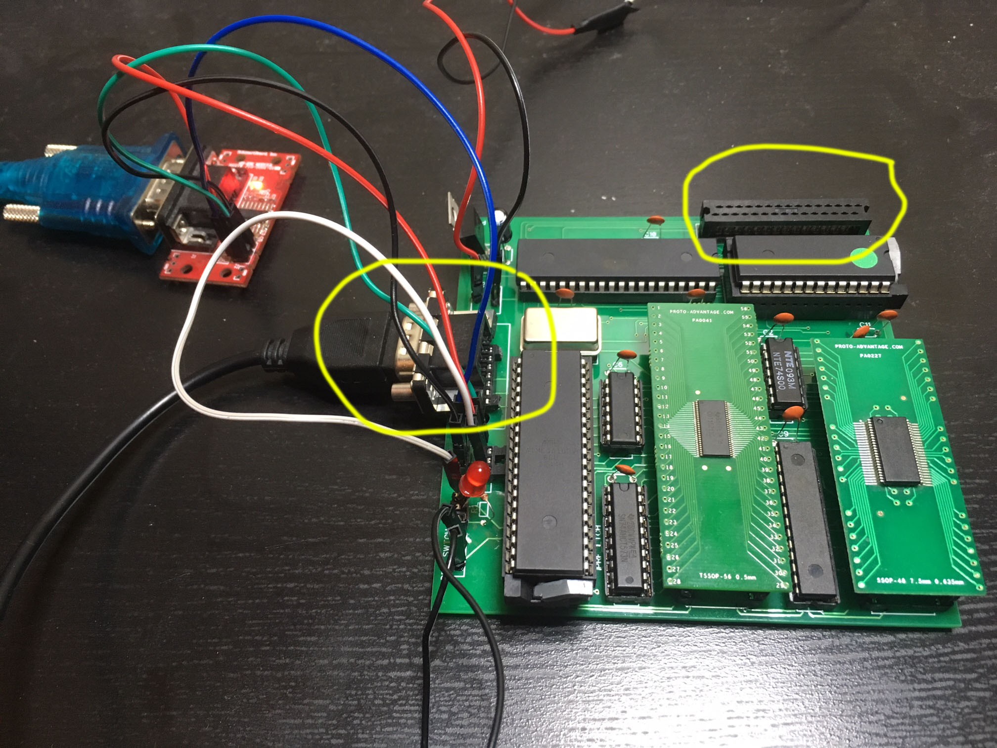
Cleaning Up
05/25/2018 at 05:28 • 0 commentsNow that the PCB worked, I decided to take a quick breather and do some cleanup. I ordered a DB9 connector and a connector for the gfx adapter which will be used for the graphics expansion board (I'll be starting on that next).
I circled both of them in yellow...
![]()
Much cleaner now! Also, it's more sturdy - I no longer worry a wire will just pop off. I also used this opportunity to add a socket for the LED light so it's not directly soldered into the board.
Next up will be to pause this and start on the graphics board!
-
We docked! (It works!)
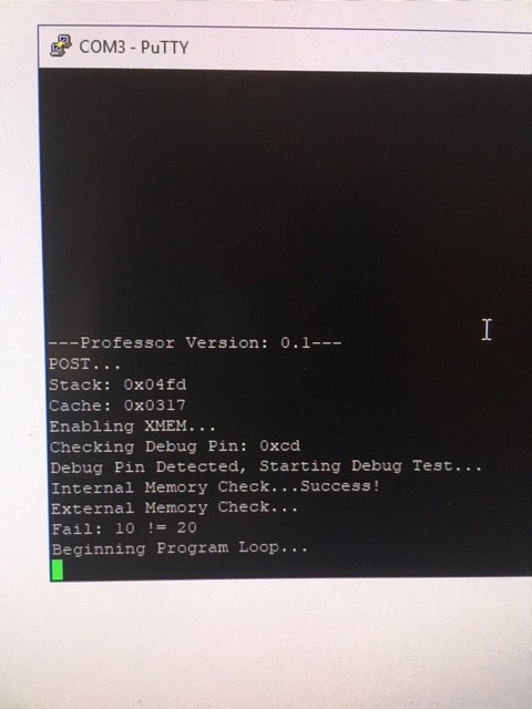
05/15/2018 at 16:24 • 0 commentsAfter turning it on and off many times I noticed it was always failing on the same external memory test number: 10.. What did 10 mean...
My external memory test routine is very simple, it writes an incrementing number (starting at 1) to the external memory addresses 0x200 to 0x2ff. Then it reads them all back, if it reads back the same numbers it wrote then it assumes success.
10 means it successfully read back 0x200 through 0x208 (values 1 through 9) and then failed at 0x209. 0x209 in address lines is 10 0000 1001 meaning A0, A3, and A9 are hot. The value 10 in data lines is 1010 meaning D1 and D3 are in use.
So I started down the path of verifying the ratlines and solder points for these were all valid. They were, but in my experimenting I discovered I wasn't getting consistent resistance readings (using my multimeter) with D4 and D7. I tried for quite awhile to reconcile this with my expected D1, D3, A0, or A3 being bad - but I couldn't come up with any logical reason.
Then I decided to remove the Professor (ATMega chip) and make sure the solder points on the bottom of the PCB went all the way up to the socket we soldered to the board. Again, that was fine.
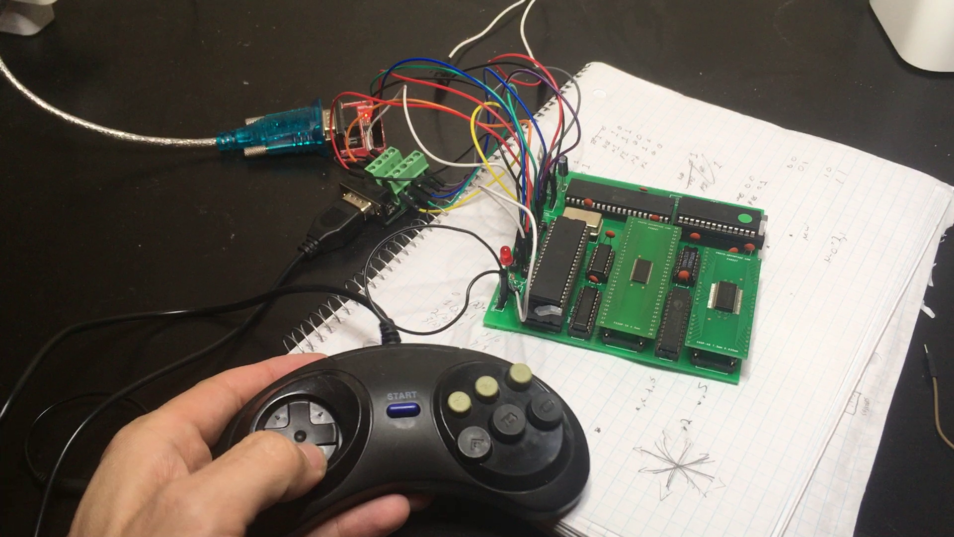
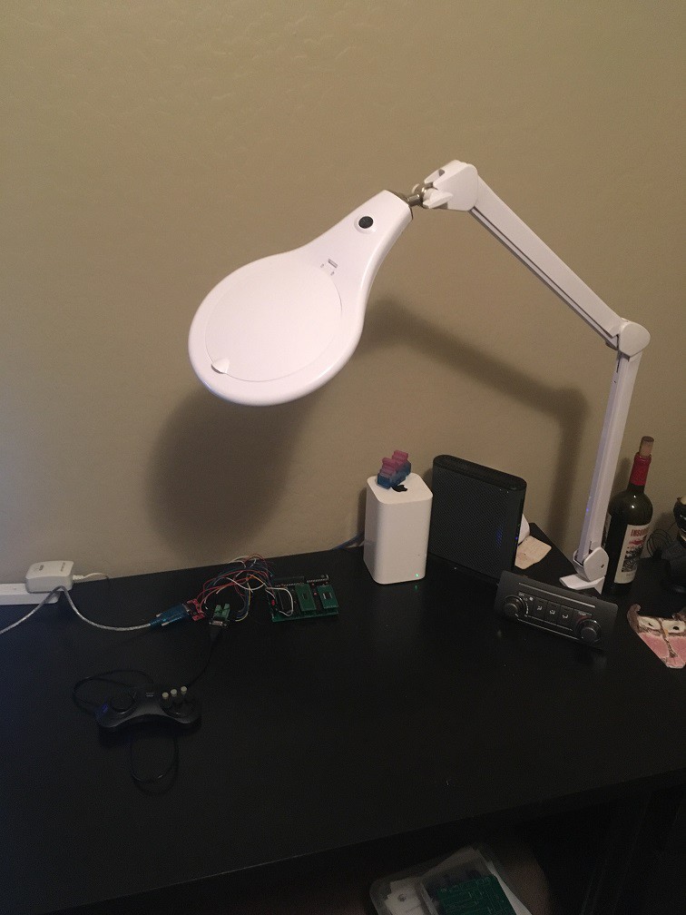
However, when reseating the Professor I noticed some of the legs didn't seem quite right...like maybe they bent at an angle and didn't go through the socket (I should have taken a pic). So I took great care to straighten them all again with needle nose pliers and tada!, it all worked!!! The ATMega shares address and data lines on the same pins - so I'm guessing some of them were bent and never made it in the socket correctly.Here's me testing it out...notice I'm pressing down on the D-Pad
![]()
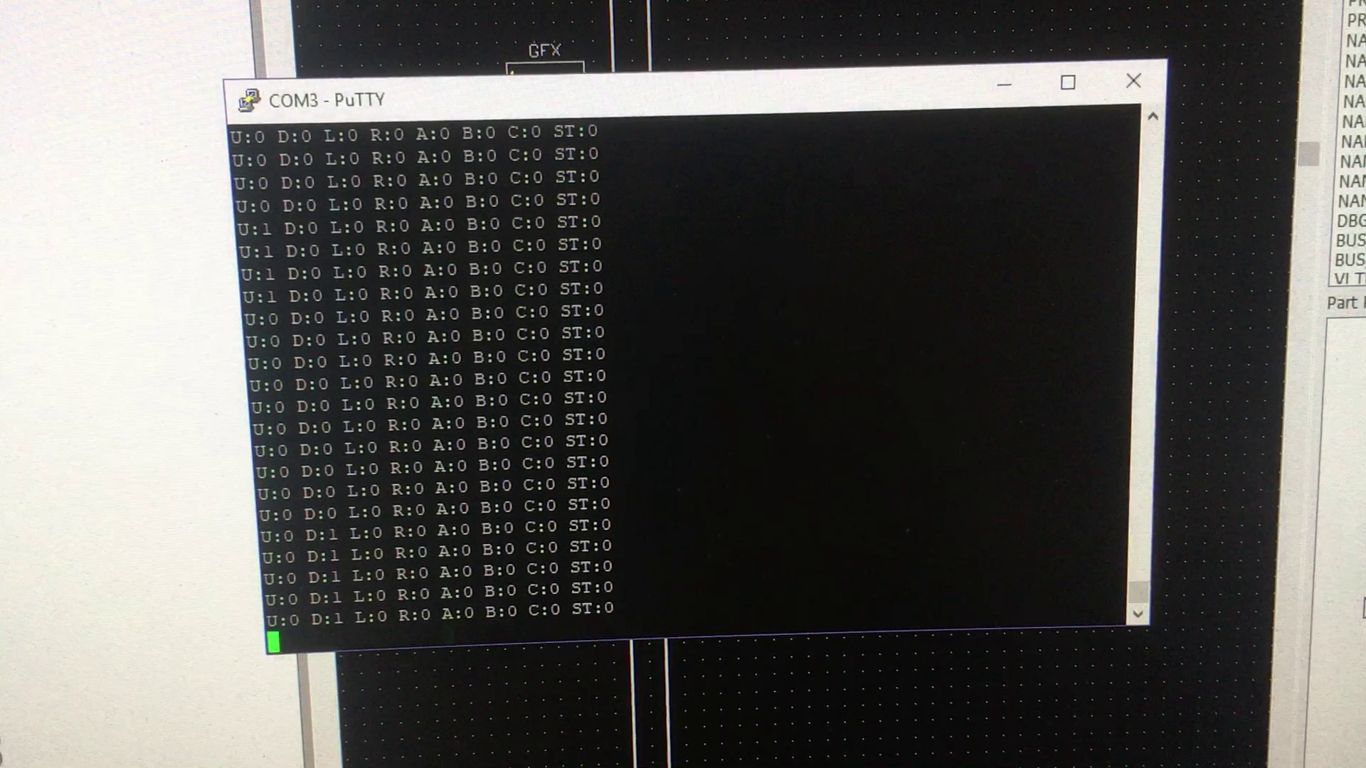
Here is the serial terminal app (Putty) reporting it correctly! (The D for Down is at 1):
![]()
btw - a quick side note, I ordered this awesome LED soldering light / magnifying glass off of Amazon, it made checking the soldering points much easier! https://www.amazon.com/gp/product/B010TOTT58/ref=oh_aui_detailpage_o00_s00?ie=UTF8&psc=1
![]()
Next up is to get the real IO connectors soldered on for the joypad, serial out, and gfx expansion.. then I'll switch gears and start working on the graphics board!
-
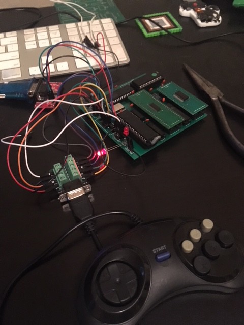
Rough Shores (Kinda but not really works)
05/10/2018 at 06:40 • 0 commentsWell I hooked it all up, to be honest I expected it to completely fail; instead, a tiny bit of it works. Initially the LED didn't blink, the board looked dead, and the serial terminal on my PC was blank. I was quite sad. Then I thought - perhaps I messed up the pos/neg when I wired up my wall wart plug to the board, so I swapped them. The LED still didn't light up, but I glanced at my computer and the serial terminal showed data!!! Specifically the Professor reported he started up but had an error accessing external memory. This was huge, it wasn't a total failure!!!!
![]()
For those of you not aware of the Professor - it's the 'smart chip', an ATMega 162 which handles peripherals, outside communication, etc. At the moment Gilligan (the 6502) communicates to the outside world via some shared RAM read by the Professor. So, if the Professor can't access external memory, it has no way of talking to Gilligan - so I really have no idea at the moment if Gilligan is working or not. I need to solve the Professor external memory problem first.
However, ignoring Gilligan for a second, if the Professor started up why isn't the LED blinking? It took me a bit of multi-meter debugging to realize I soldered in the LED backwards... totally my fault, I designed the schematic to the wrong pins. So I laid a second LED on its side with the correct legs touching and it blinks as it should!
![]()
So what's next? I need to figure out why the Professor can't access external memory. My guess is it's either a bad solder or another messed up line on the schematic. I'll be checking both over the next few days - I'll report back when I find something!
btw - I need a bunch of jumper wires to hook everything up securely, I ordered these on Amazon:
https://www.amazon.com/gp/product/B073X7P6N2/ref=oh_aui_detailpage_o08_s00?ie=UTF8&psc=1
-
Land Ho! (Components are Soldered)
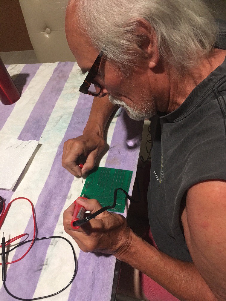
05/09/2018 at 16:26 • 0 commentsThat was much longer of a delay than I anticipated, but I was finally able to coordinate with my dad and get everything soldered to the PCB. Why my dad you might ask? His soldering skills far eclipse mine and I didn't want bad solders to be a factor when I plug the board in - you see I'm afraid it won't work initially, most likely some step I will have missed when translating my bread board wiring to the diptrace schematic..I tried to be thorough.. but this is my first time and all.
The next step will be to wire up the DB9 joystick connector, RS232 output (serial output), and the power.. then we'll see what happens! I'm planning to get to that tonight. Man I'm excited! But, I have to get back to my day job now - so I'll leave it at that. Below you can see pics of the final solder job!
Here we are getting started...
![]()
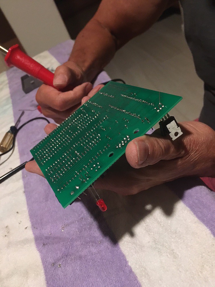
Here's the bottom - all finished!
![]()
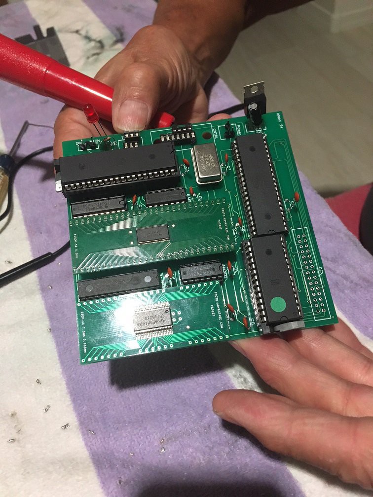
And here's the top! A thing of beauty, he's such a stud!
![]()
-
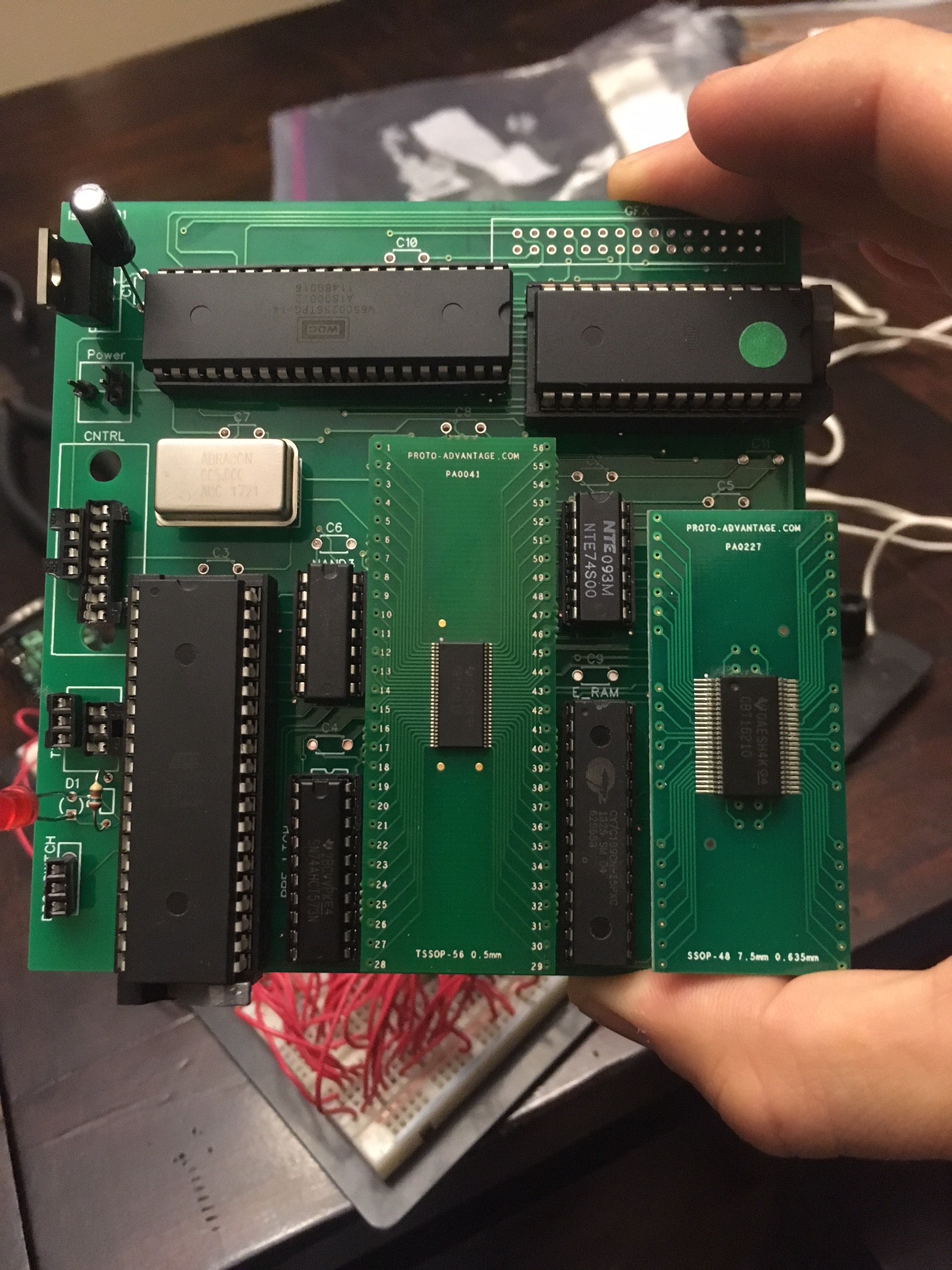
Onward to the Sea! (Everything Fits!)
04/26/2018 at 05:49 • 0 commentsWell - I spent tonight putting all the chips in, everything fits! To be honest I was a bit shocked... I'm still not totally expecting it to work - but I'm more hopeful than before.
The next step is to solder it all in, I'm pretty poor at soldering but fortunately my dad is a stud at it, I'm going to bring him over Saturday to help me out.
Why Saturday? Well - turns out I didn't have the bypass capacitors I needed, so I just ordered those and they'll be here Saturday.
Which brings me to yet another area I'm not familiar with... what should the value of a bypass capacitor be? I did some light research tonight and found some various formulas and calculators - but I wasn't clear on the inputs (e.g. what the heck is my 'emitter resistance'). However the consensus seems to be .1uf will be enough. That was further validated when I found this sheet on http://www.nerdkits.com/forum/thread/1598/:![Bypass Capacitor Values]()
and hey - if it's on the Internet it must be accurate right? All joking aside, I'm running at 8mhz so if this is accurate .1uf is indeed fine. I'll do more thorough research in the morning but the capacitors were cheap enough for me to take a risk and order tonight. I'll post an update when I figure out the definitive answer for calculating the correct value.
So - without further adieu, here it is with the chips in! (Technically the chips are in sockets, and the sockets are in the board - this way I won't ruin the chips if the board doesn't work).
![]()
-
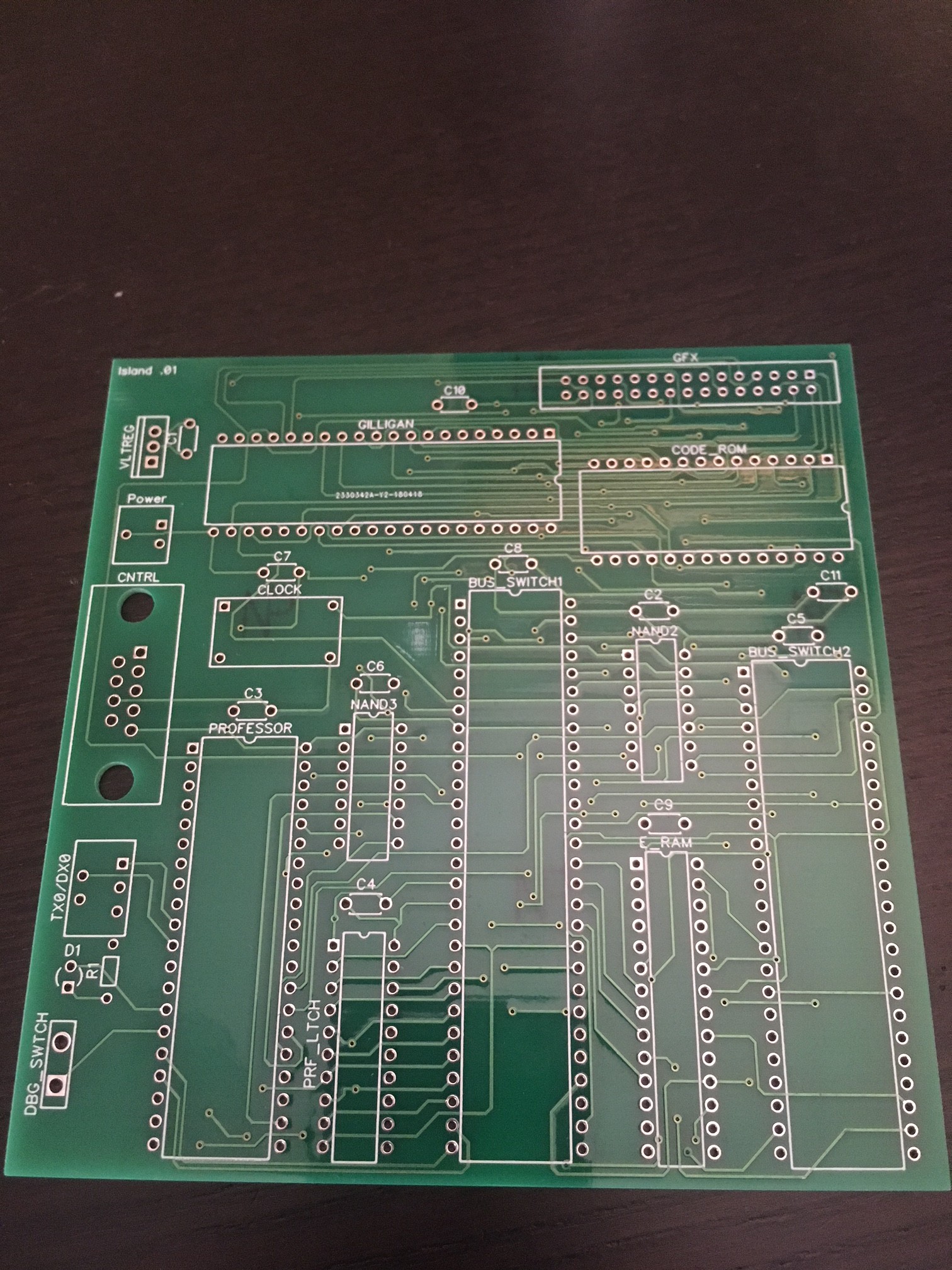
The Leak is Patched (new PCB arrived)
04/25/2018 at 17:14 • 0 commentsMy new PCB has arrived (see below) - it all looks correct ... but we'll see. My next step is to place all of the sockets and make sure I didn't mess up any other measurements. I'll post when that's complete.
Also - I discovered that diptrace has the part numbers for the different components I'm using, and I can use those part numbers at digikey.com to order connectors which plug into the PCB. For example, the connector I'm going to use for power can be found here:https://www.digikey.com/products/en?keywords=52004-0310
The status.md on my github currently has a "parts" section with links to the parts I plan to order.
This will take a lot of the guess work out of finding the right connectors for parts of the board which require external connections. But I'll wait to order those until after I've verified that my design is correct and the board works :)
![]()
SS Minnow - 8-bit Game Console
Building an 8-bit game console based off of the 6502 and an ATMega 162 (for advanced I/O) .