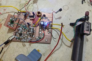
I am designing and building an off-line 30V, 5A Variable Lab Power supply. The following design features will be included:
1. 0-30V , 5A single ended output.
2. +-12V, 1A split.
3. 5V/3.3V/1.3V output.
4. Necessary protection methods for undervoltage, overvoltage and other faults.
The design will consist of an SMPS stage that steps down the rectified DC voltage and further linear stages that provide the constant voltage/constant current outputs. The 0-30V variable output will be directly taken from the SMPS stage with appropriate filtering at the output.
This is a complex project with lots of sub domains that may take their own time to design/develop. Along the way I intend to become proficient in designing switch mode power supplies.
Components
1×
IRLZ14
MOSFET Transistor, N Channel, 10 A, 60 V, VISHAY.
The main output inductor after the catch diode is the focus of this design process. I had calculated the of this part using an empirical formula given in the Power Supply Cookbook by Marty Brown , but felt that the estimate was not mathematically sound. So, I searched around and found an app note by TI, AN- 1197. This has detailed mathematical calculations for output inductor calculations.
It has a nice little mathematical algorithm for output inductor calculation geared specifically to buck converters. Lets see where it goes.
Another hurdle that I face is that there seems to be an inverse relationship between the current carrying capability of off the shelf coils and their inductance. The largest current rating I could find for an inductance of 100uH was 3A which is less than the average inductor current and wont work.
Also, I had calculated the inductor current ripple based on an estimate, which I have now discarded in favor of a superior method described in the app note.
I have selected the majority of parts for the switch mode unit. Now I am stuck on magnetics design and it is proving to be more difficult than I initially thought. The topology I have selected for this unit is a forward-mode buck converter, the selection for which was based upon an app note by ON Semiconductor that I have uploaded to the project files. The main motvation behind doing so was the simplicity of the buck converter as compared to the other option- the flyback converter. Simplcity here is a relative term.
The semiconductor switches and the related control ic's have been selected. Discrete compenent selection is proving to be difficult as the guide I am following for this design has a cookbook format and the estimate equations for the output choke are approximate at best. Also finding appropriate magnetic elements is proving to be more difficult than semiconductors and ic's.