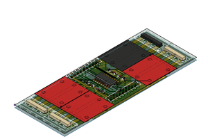
• Planning modularity

    Ekaitz Zárraga12/10/2018 at 12:11 0 comments

    Hey!

    Time to go on with this... Ok.

    Modularity is key in these kind of projects. I don't want to spend ours and ours routing a big PCB and then realize a small piece is wrong. That's not for me.


    So, the idea here is to create small parts that we can certify they work independently. As the motherboard depends on two big components, let's make the modules according to that:

    • Switch from one side
    • Compute modules for the other

    The first point is to make the switch work with no problems. We can reduce the size of the prototype's PCB drastically if we create an independent switch board. Once we have that we can test it and then make the Compute modules connections to the main switch board. We have to be careful with the connectors we use there because they can corrupt the Ethernet signals and screw up the whole thing.

    From the side of the compute modules... It'd be nice to have the chance to connect other kind of compute modules, but we can't expect all of them to have the same DDR2 pinout. We'll stick to the Raspberry Pi CM3 one at the beginning but it looks like we should make something to change this. One of the options is to keep the motherboard separated in the two parts so we can use the same Switch board with different Compute Module boards. The compute module board must have all the necessary connections for the Compute Modules to work and expose the necessary pins: all the Ethernet connections, and the power source connection...

    So, the first point is to make the Switch work 100%, and then go expanding PCB with the other module. We can insert the switch in a PCB that is soldered later on the final one, like the  RN4020 does. With that design, we can even distribute the Switch board independently for others to use it in their projects, and then go on with the CM part.


    I don't know, we have to start somewhere, don't we?

  • Ethernet connections for an amnesic Telecom. Engineer

    Ekaitz Zárraga08/18/2018 at 15:34 0 comments

    Yo!


    Don't worry, the title is for *me*. I'm a Telecom Engineer but I spent most of my career working with software and I almost forgot the signal+electronics part.

    Let's take a look to all this thing.

    If we simplify, we can say the motherboard here is just a switch with some connections to computers, everything well routed in a PCB. Nothing else.

    So, the connections with the Switch are made via Ethernet. I chose a switch from Micrel (now part of Microchip) called KS8999. The switch is a 9 port switch, 8 with PHY and the other with MII.

    First of all, what does that mean?

    It means 8 of those ports are PHY-sical and the other one is a Media-Independent Interface. The MII interface is supposed to be the connection to the WAN (the external connection) and the others are supposed to be to connect the computers of the cluster to them.

    The difference between them both lays on the abstraction level they have (directly related with the OSI model). The PHY ports directly handle all the media specific details, they are oriented to signals more than to the Data. The MII interface is supposed to need a PHY device to handle the low-level and media-dependent parts of the connection while they strictly handle the data interchange with that device.

    As this project aims to connect devices via PCB and not cable, some considerations must be take in account, the connection between devices must fulfill the conditions imposed by PHY devices. They expect some impedance and stuff, if we change that, the reflections and stuff will destroy our signals and the PHY devices are going to be unable to extract any data from them.

    All of this stuff has any sense?

    Going to the detail, "normal" ETH connections have a cable in there with some RJ-45 connectors being the interface between the PCB and the cable itself, right? The RJ-45 connectors and the standard configuration has some transformers to provide isolation. But in the PCB we are not going to use them. Also, the cable and the connectors have specific inpedance and attenuation requirements. We have to take them in consideration for the PCB layout and connection.

    We are going to make simple connection with some capacitors and resistors.

    There's a good application note by Micrel for that:

    ww1.microchip.com/downloads/en/AppNotes/Capacitive Coupling Ethernet Transceivers without Using Transformers.pdf

    The MII interface, which will be used for the external connection will be made in the standard way with an RJ-45 connector because it's supposed to be connected to a router or something.

    This AN is also interesting for the signal routing:

    http://ww1.microchip.com/downloads/en/AppNotes/General%20PCB%20Design%20and%20Layout%20Guidelines.pdf

    From the side of the Compute Modules, they are probably connected via USB because they don't have any ETH port. We can use a USB to ETH device for that, like the Microchip LAN9512 or similar.