The 74's called ... (SUBLEQ)
Yetanother simple CPU of TTL chips.
Yetanother simple CPU of TTL chips.
To make the experience fit your profile, pick a username and tell us what interests you.
We found and based on your interests.
The Full adder ('283) is placed in top row, plus an inverter for the Breg input, so it becomes a SUBtractor. The IOD (the I/O-detector, previously called ZER) signals on all-1's on the XFR-register output.
Placed, but not yet wired, is the LEQ detection on the SUB output.
Of course, I had to test this interim stage, before having done the LEQ. I loaded 4, 5, -1, 5, 3 into the RAM, and then microstepped and verified that all the expected lights lit up. Thus it did one SUB(nobranch) instruction, and the correct numeric result. Yes ! Wave !
Onwards to wiring up the LEQ and then need to write tiny test programs. Thinking, "read INP and add it to running total on OUT". Oh, no conditional branch in that. Hmm... I only have room for 4 instructions and 3 variables
The Halt is not done, and I have to think how it should stop the clock.
So far it is a 4 bit data/addr. There is room (in the blue boxes) for the chips One counter, one Adder, one inverster one OR gate) to make it 8bit as soon as the 4bit is working. The Bus-display needs widening, too. But before that, I'll do an Arduino "interface" so I can load RAM with program. Toggling in with the Load button gets tedious real quick.
Another "minor" rework of the controlsequence logic. I just stared hard at the logisim circuit long enough, tweak and simulated and found a way to free up 3 gates, even with the additional constraints included. I also managed to reduce the wiring mess, a little.
ToDo: include some logic to reset the sequencer in the non-branch case or indeed skip the 8th step as it is a 3bit counter.
The A1 etc refer to chip/gate. (The inverters top left do not exist in the real circuit, only in the simulator, beacuse the signal is active low, so the Input buttons are easier to work with as active high.)
I now unconditionally copy Register A into Result (what 2nd argument points to) to test my write back.
The "bus" in the middle will have LEDs for all 24 lines, when I get to a CPU project with 8 data 16 address. At the moment 4 bit databus.
I have reaaranged a little (as described in previous log) but I am NOT happy with the layout as a whole. Implementation is "organic growth", but I do not want to rearrange everything or every step. The jumperwires are for temporary fixes (like LEQ tied low, as there is no SUB to generate the signal yet, but I can still test how it would work on the µ-sequencer)
At this point I discover a few (more) errors in the design <sigh>
| Units | Signals | ||
|---|---|---|---|
| RAM | Memory | ADDR | Address to memory |
| SEL | Select address source | DATA | bidirectional data (a bus) |
| INP | Input, currently DIP switch | SXP | Select XFR or PC as source for ADDR |
| OUT | Output Buffer (goes to display) | LDP | Load PC with new value |
| XFR | Transfer Buffer, for the indirect arguments | INC' | Increment PC |
| PC | Program counter | IOD | Input/Output-Detect, ie address is -1 |
| Areg | A register | LDX' | Load the XFR register |
| Breg | B register | DOD | DataOutputDeny (=not RAM on Databus) |
| SUB | Subtraction unit | WRE | Write Enable |
| Notes: In these schematic the signals are all positive. (In the circuit half are negative=true) The '-mark is for edge triggered (otherwise they are static levels) | ENI | Enable Input (INP on databus) | |
| ENR | Enable Result (SUB on databus) | ||
| LDA' & LDB' | Load A and B register, respectivly | ||
| LDO | Load Output Register | ||
| LEQ | Less-or-Equal result in SUB | ||
Signals activation by step above the box, with hollow arrows show the alternative on a condition being true. The listing shows data flow, and the last is the special event when pressing the "load"-button (two pulses generated, not the clock)
Microsequencer-clock-"decoder"
This shows the complex truth with negative/positive and static/edge logic mix. The output suffixes mean "~"inverted, "+"ve and "-"ve edge. The LD1 and LD2 are the two pulses from the manual Load button. The counter reset takes away the 8th redundant µstep, and I should do it for the nonbranch 7th step, too, but I've run out of room for more gates.
in the probable order
And when it runs, extend to 8 bit data/addr and loading of programs from Arduino
Progress is getting easier. I now have the XFR register working, and verified that indirect addressing works. YEAH! There was a debugging session - now that I needed to load the RAM with data, I discovered that the data was not loaded in the correct address. Finally (with a help of a Saleae logic analyzer) I had that Doh! moment - the monostable generating the LD1/2 pulses (you can see the capacitors on the picture) was wired wrong and fired LD1 and 2 at the same time, instead of after each other. Now the manual load works as advertised
Then there was a challenge with the PC jumping ahead 3 adresses when going from 7 to 8 - it turned out the LoadCounter line was floating (the LDP signal is not hooked up yet). It proves again that ALL inputlines to a chip must be tied High/Low if they do not have a signal. Of course I knew that, I was just being lazy/forgetfull/optimistic.
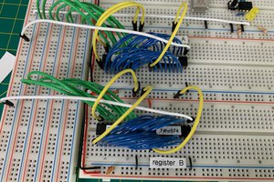
Hooking up the A and B registers was trivial, and the readout is temporary, just to convince myself that I load them with the indirected content.
Next is placing the ALU, where A/B display is. I'll use the '283 simple adder, and inverters to make it a subtraction - 2 chips (4 for 8bit wide. Note the room reserved for extending SEL and PC when going from 4 to 8bit). The LEQ detection is challenging me trying to minimize chipcount to do it.
It is getting tight on breadboard space. (I have more of them, but I'd rather not) Planning to move the INP and (not yet constructed) OUT unit to the left. That places all human I/O on the left, and right is Internal, I thus will use the "bus" (the strip board i the middle), and it is planned to have LEDs on it, too, so that removes one of LED bars. I had sort of semi-planned not to use "bus" in SUBLEQ ("only" ENR and INP (and RAMdata) are tristate) but that's the fun or point of doing a project like this - challenging the loosly laid plans to deliver in RealLife.
The Microsequencer is causing gnashing of teeth. ( I've updated the diagram/tables in previous log wit the corrected correction fix, revised. )
But now most signals work - ie they match my intended flow from the post "Block diagram". Time will tell if that works.
Still missing is LDO and LDP signals, but they're easy.
Actually I only wanted to test the Manual Load circuit, where two monostabes trigger the Input latch and a write to the RAM. They would need to go through some sort of "OR" operation wit the signals from the MicSeq which would generate the same signals under some conditions.
Originally I thought the MicSeq would be dead easy, as I had one (negative) logic line for each step, and a simple OR or AND would be enough for where a condition is needed. Like, "Increment PC on step 2 and 4 and on 6 if LEQ is false". But, the 74LS138 has a negative signal, and most registers trigger on an edge and need delaying until the RAM output has stabilised (ie can not trigger on the same edge). That is handled by AND-ing in the clock, so I get two edges on one step.
Note: Where it says "Seq" in the table it that step, ie Sequence5 in the ENR(EnableResult) column. I've tried to factor where I can but it still ends up with 26 gates on 7 chips (using triple-input gates doesn't help the chip count) ! And this is not even a proper instruction decoder, as there is only ONE instruction. Sigh. Defenitly will be using a EPROM in the future, but for now I wire this up. Suddenly I get worried I will rewire countless times as I discover errors, so I start using LogiSim and yes ... errors. The above is the corrected version, and below the circuit. (yeah, I could format it prettier, but that's not the point here)
If you trace backwards you can see that DOD (RAM DataOutputDisable) is simple, only one OR and NOT gate, but that the LXP (Load the indirect address register) is 5 gates.
I'll think I start with the Program Counter. It is a counter. I happen to have a lot of 74LS197 (salvage from a surplus store) so I use one (or two) of them.
4 bit counter. I use the Arduino tester, to verify that I truly understand the chip. It actually is two counters; one single bit, and one with 3 bits. There is NO CARRY. OK, as the count clock is negative-edge sensitive it simply means putting the highest digit of the previous stage into the clock of the next counter.
The Clear will go to the global Reset line.
It will be another 74LS197 counter driven by the clock going into the 3->8 decoder 74LS138, where one of the 8 lines is high low for each tick. Route to each latch/tristate, with inverters, as appropiate. I hope that the "random logic" to get things happen at the correct clock edge will remain reasonably simple.
The microsequencer works as advertised, ie one of each of the 8 controllines go low at the desired step. (The rest is not on the above picture:) The PC gets the INC on step 2 and 4, and conditionally on step 6. Currently 4 ddressbits cycle correctly, address the RAM, and data can be stored and retrieved (for now by manually setting datalines and manually toggling WriteEnable). It is a 4bit machine for this phase, and the LED bar shows address and data.
The button debounce is giving me headaches - I cant get 100% releiable single step, and I do not know if reason is the button is too bad, the breadboard gives way/glitches, or I have stray signal pickup. (The latter seems likely - I sometimes get a "step" when touching some wire). It will do for the while being.
(Some while later): Clock works. The PC increments as it should at right microstep, including a manual simulated LEQ branch (ie do not increment, but the jump isnt there yet). Also the RAM access works. A manual (moving jumpers) load of data shows that read and write work.
The green display is temporarily both 4 bit address and 4 bit data. (Everything is 4 bit for the while being)
I think I now have the right block diagram. The first one was easy, took 5 minute sketch, the SUBLEQ is sooo easy. Yeah - after thinking about it, there was an error here. Oh and an ommision here. And hey, indirect addressing on everything! "Rinse and Repeat" the design a few cycles.
Note that input and output is included as an extension to the pure SUBLEQ. There is no other instruction than SUBLEQ, so INP and OUT are memorymapped, ie addressing location 0 will read INP (switches) or write OUT (7seg digit). Edit: It is not strictly memory mapped, as referencing address zero changes the way the instruction executes, rather than redirect the address.
XFR, Areg and Breg are latch-registers, PC is a presettable counter, SEL a 2-to-1 selector, SUB does subtraction and signals LEQ. The ZER senses address zero. ENI/ENR are tri-state gates (can't seem to design my way out of using tri-state on the databus, as it is bidrectional).
This of course needs some squencer to control, the microsequencer
The last line is the Hardwired Loader - to be implemented as a push button that transfers INP to RAM, then increments PC.
It started about 3 years ago with viewing the Ben Eater series on building a simple CPU with just breadboards and TTL. Although the 74's are "relativly cheap", there are lots of them, and the total expenditure kept me back. Ben Eater sells the kit, but that makes it a boring repeat. In autumn 2019 I bought a selection of chips, both to cover that project, and a "suitable" selection of others, and a few to spare.
I want to experiment with the challenges of of doing my own. I know the architecture of CPUs as such, so this is purely fun, as a puzzle. I want to extend the BenEater design with more RAM, an IO subsystem (keypad input, Serial?), something to load RAM, Interrupt handling, and paging. Of course at that point it isn't a "simple CPU" anymore.
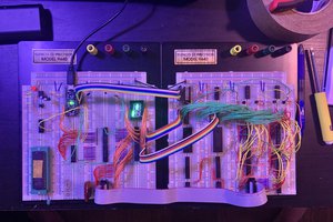
As the title picture shows, I have constructed a tray so I can easily take it out to play, and put it back even in mid work. On a wooden base I have a large conductivefoam area to store chips, there is a 5V supply, and an Arduino to act as a test generator, and bulk storage IO device. Breadboards obviously, and a strip-board bus in the middle (rather than using even more breadboard)
"Walk before you run" - so this first project on my CPU constructor kit simplifies CPU capabilities even further: One instruction, avoid "bus"/Tristate, start with 4bit (address and data).
Create an account to leave a comment. Already have an account? Log In.
It is early in my project, but the OISC does not define "addressing modes". I was staring at the ceiling and wondering if Immediate operand could be included without violating the OneInstruction. It would not make much of a difference SUBLEQ A, B, C could be SUBLEQ #A,B,C (except run faster?) but there are more possible addressing modes (I cut my teeth on the PDP-11 with 7 addressing modes ...) Either way it would be after the basic model does what it is supposed to do.
M²
You can add another OpCode (use the most significant address bit as an OpCode flag) but generally you use self-modifying instructions. Trust me, it does your head in. If you are young, no doubt you can do it but after fifty it is like banging your head against a wall. But of course self-modifying code needs to be loading into RAM, and that needs code in ROM to load it. This is the Basic/Primitive OS I spoke of earlier.
Here is a cut and past from my log on self-modifying code
==================================================
Self Modifying Code - Part 1
---------------------------------------
SUBLEQ can use pointer but it requires the use self modifying code. Reading data from a memory location to a variable called DATA from an address stored in (pointed to by) a variable called ADDR is an example. We can write it as:
DATA = [ADDR]
Not to be confused with copy or move:
DATA = ADDR
DATA = [ADDR] can be coded as:
T T ? ; T=0
PTR PTR ? ; PTR=0
ADDR T ? ; T=-ADDR
T PTR ? ; PTR=ADDR
T T ? ; T=0
PTR: T T ? ; T=-PTR (self modifying code)
DATA DATA ? ; DATA=0
T DATA ? ; DATA=[ADDR]
Although the assembler thinks the first T on the PTR: line is real and initially set with the address of "T", the code above overwrites the address with the value held in ADDR. The only problem is that code cannot reside in ROM (as it is self modifying).
A more general form would be:
Copy [SRC] to [DST]
This would be coded as:
SRC_PTR SCR_PTR ? ; Copy SRC to SRC_PTR
T T ?
SRC T ?
T SRC_PTR ?
DST_PTR DST_PTR ? ; Copy DST to DST_PTR
T T ?
DST T ?
T DST_PTR ?
NDATA NDATA ? ; COPY [SRC] TO NDATA TO [DST]
SRC_PTR: SRC_PTR NDATA ? ; SELF MODIFYING CODE
NDATA DST_PTR: DST_PTR ? ; SELF MODIFYING CODE
T T RTN ; RETURN
Getting code in ROM to RAM without self modifying code is tricky.
---
I did warn you that self modifying code will do your head in!
AlanX
Welcome to the dark side!
I designed a hardwired subleq CPU and I build a simple compiler tool train but the results were quite disappointing. Subleq is very memory inefficient:
12 lines of high level language coverts to
74 lines of OpCodes (95 words), which converts to
3126 lines of Subleq including comments (5530 words).
So the minimum address space is 12 bits (16 bit would be more useful).
Anyway, best of luck, AlanX
Which bit is Dark? TTL, BreadBoardCPU or SUBLEQ in particular? :-)
Thanks for the heads-up, SUBLEQ will remain a testbed exercise, 4 bit or 8bit, before I "clear the board" and do the next one.
I know very little about making a proper toolchain, but for SUBLEQ I have made a simple python assembler-and-simulator.
M²
Become a member to follow this project and never miss any updates

 Yann Guidon / YGDES
 spudfishScott
 Tim Ryan
 Brandon Reinhart
SubLEq, it is evil! But breadboard runs up as a close second.
You basically cannot do anything close to useful with 8 bit. I did do a move only (i.e. TTA) CPU with 8 bit and could do something useful (i.e. a monitor program), but SubLEq is just the worst.
My tool train is in "C". I don't think anyone can program directly in SubLEq, you need to set up a basic/primitive "operating system" and use a macro style assembler.
Some of the challenges ahead are self-modifying code, the zero bug, boolean logic.
Even I/O is a headache.
I wrote a PL/0 compiler for SubLEq, there is a C compiler on the Internet as well. In the end I decided not to build my CPU design.
AlanX