0%
0%
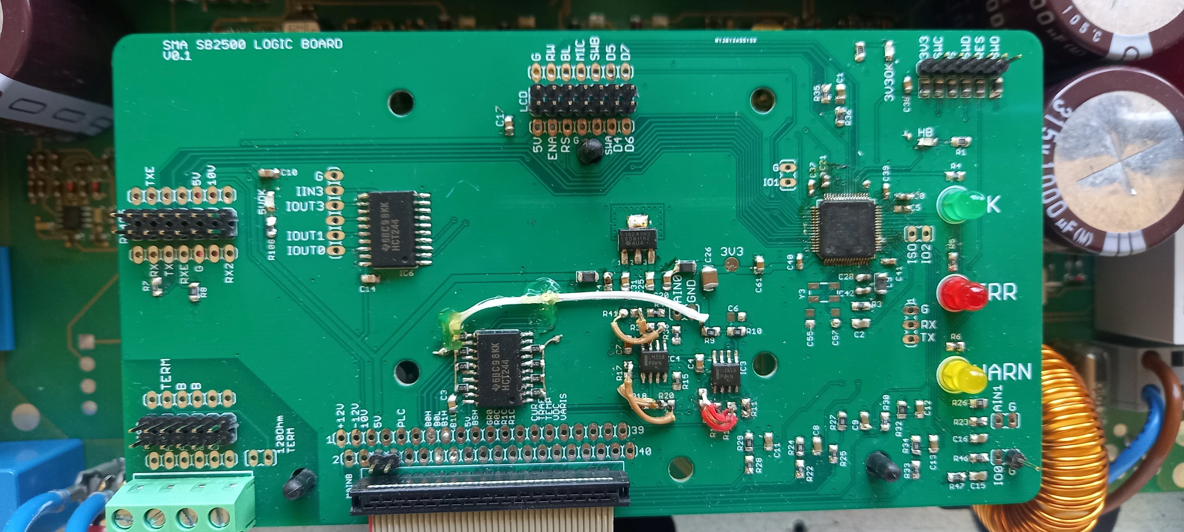
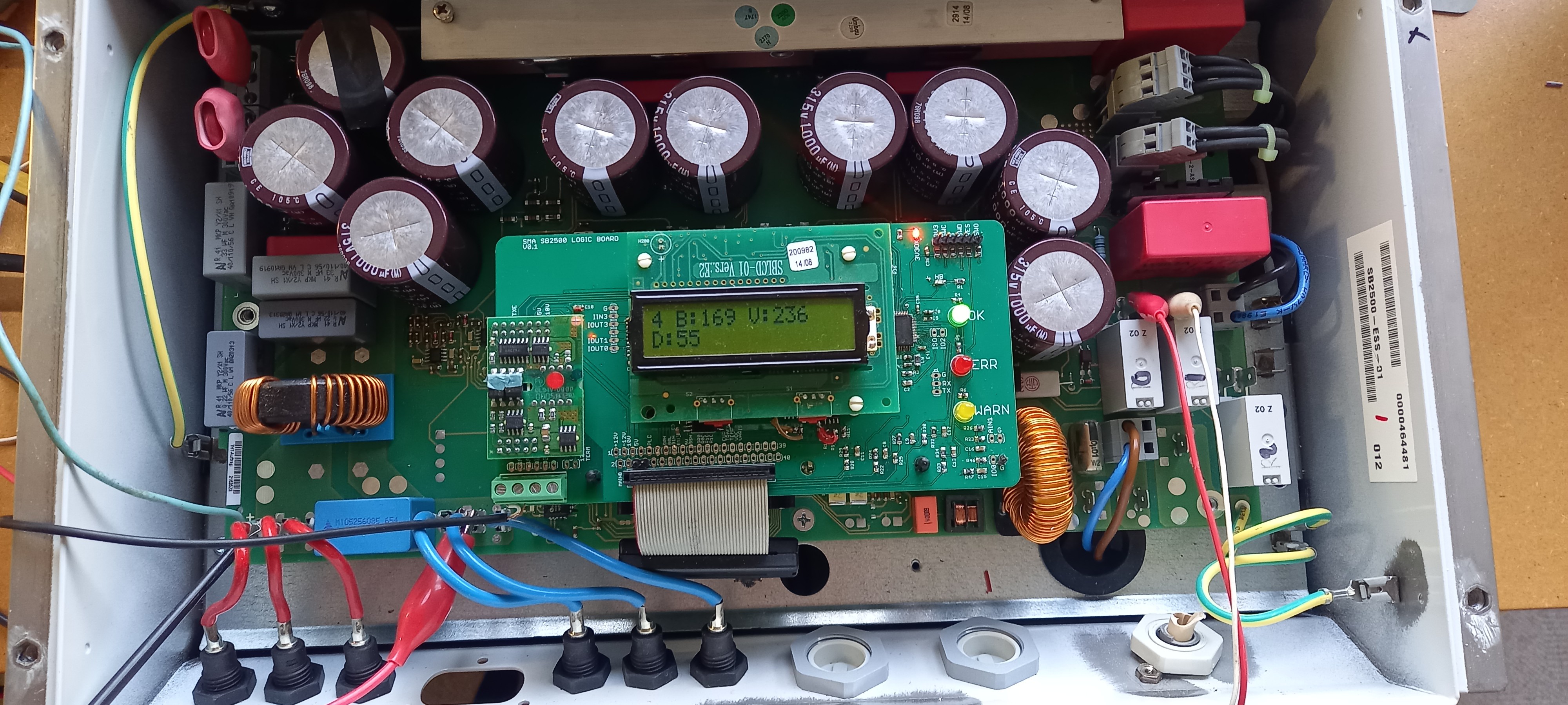
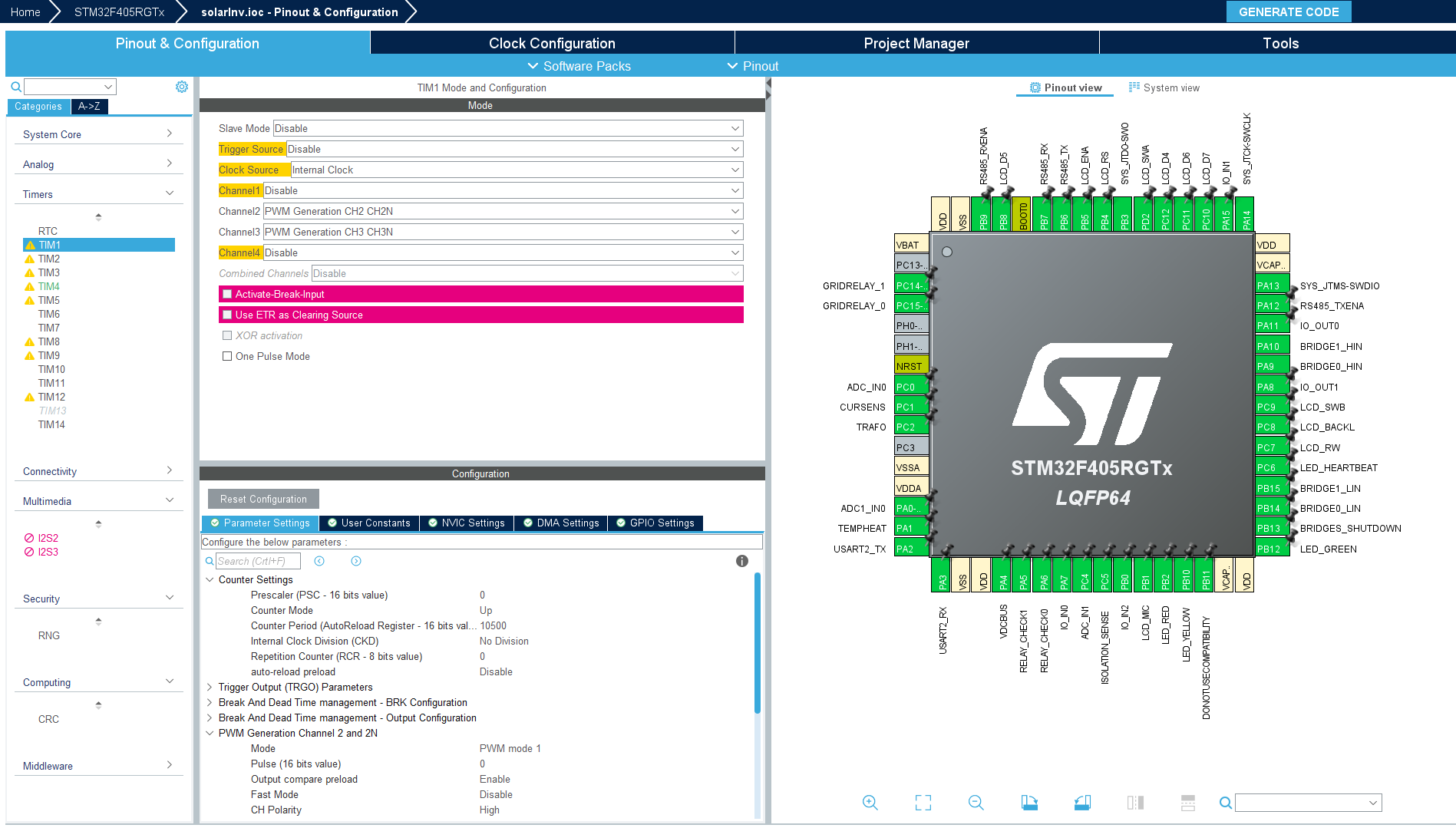
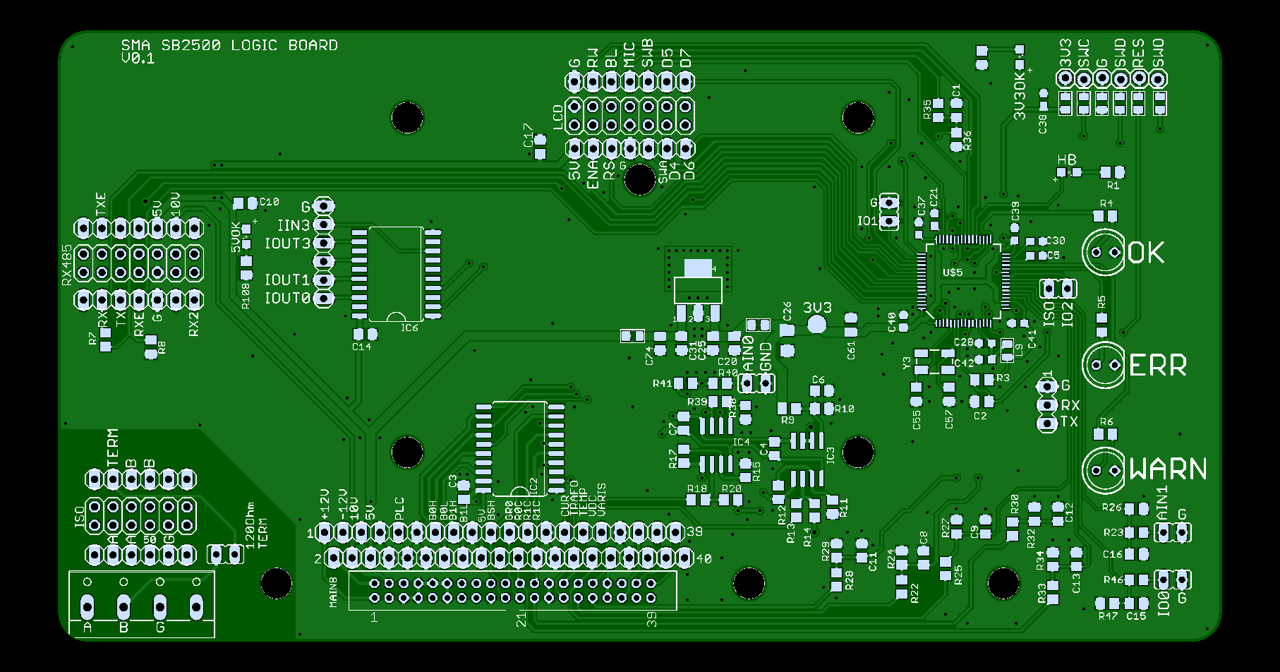
Grid Tie inverter SMA Sunny Boy SB2500 openlogic
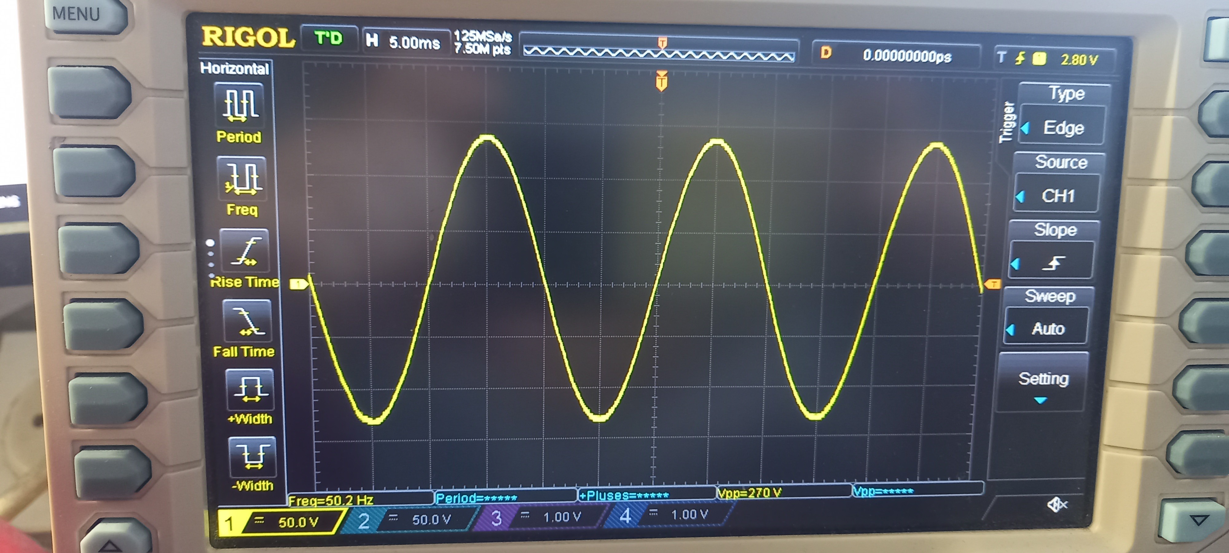
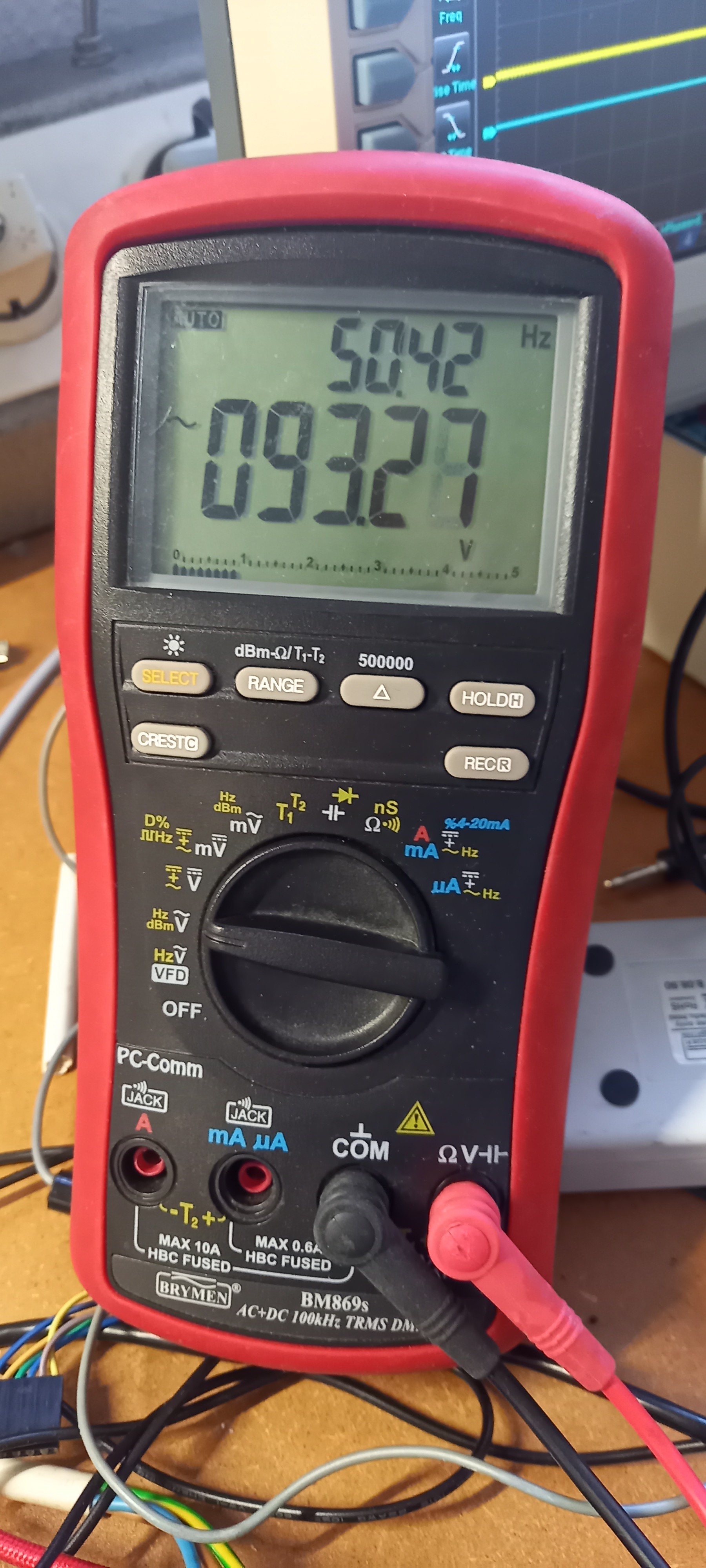
Try to reuse a SMA Sunny Boy 2500 Grid Tie inverter as an off grid inverter
 ClimbinElectronics
Become a Hackaday.io member
Already have an account? Log in.
Just one more thing
To make the experience fit your profile, pick a username and tell us what interests you.
Pick an awesome username
hackaday.io/
Your profile's URL: hackaday.io/username. Max 25 alphanumeric characters.
Pick a few interests
Projects that share your interests
People that share your interests


 sjm4306
 c.Invent
 Eric Michat
 fredkono
Hey man, DM'd you. About to do some work on my SB7000. Was wondering if we could help each other out.