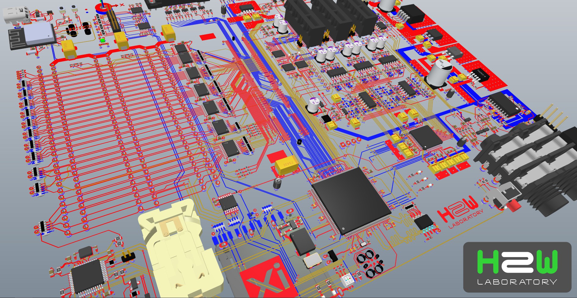
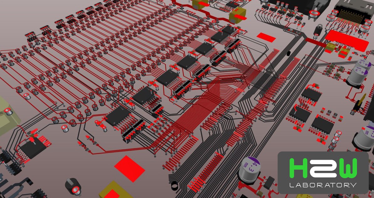
Three socket connectors, it is not a PCIe interface even though it uses its connector. It is a specialized sound synthesis bus, the details of which will be published when the development is finished. At this point things can still change.
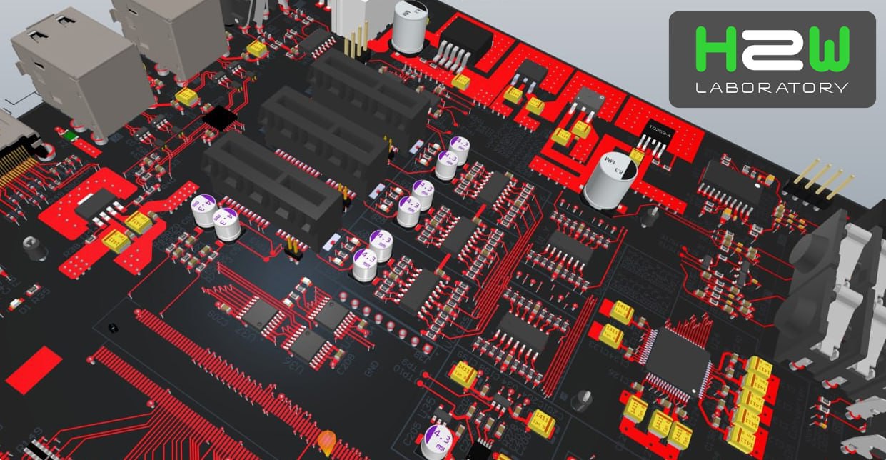
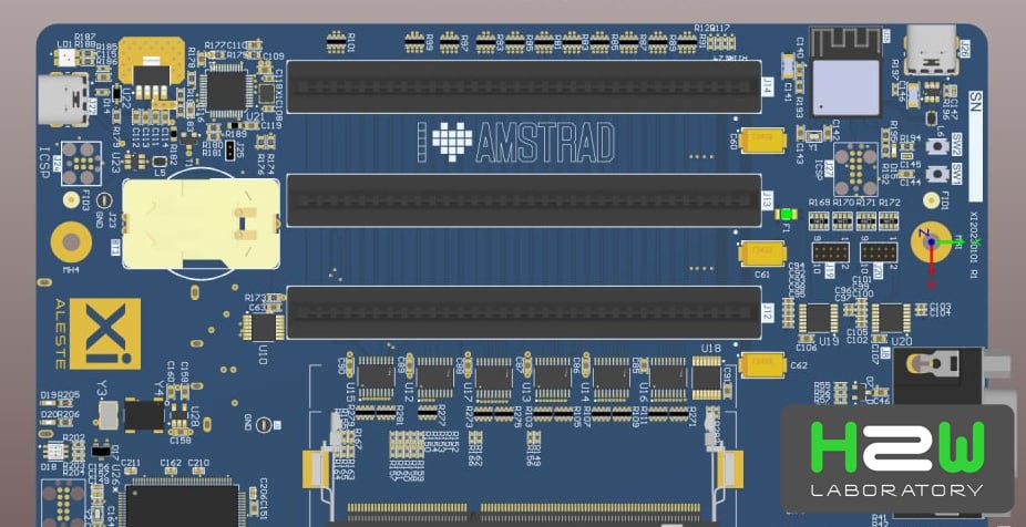
1) STLink USB 2) SWD for MCU1 3) Battery holder 4) SD card reader on the back side of the PCB. 5) DSP + QSPI Flash ROM 6) SWD for DSP 7) Reset button 8) Line input 9) Line output 10) Headphone
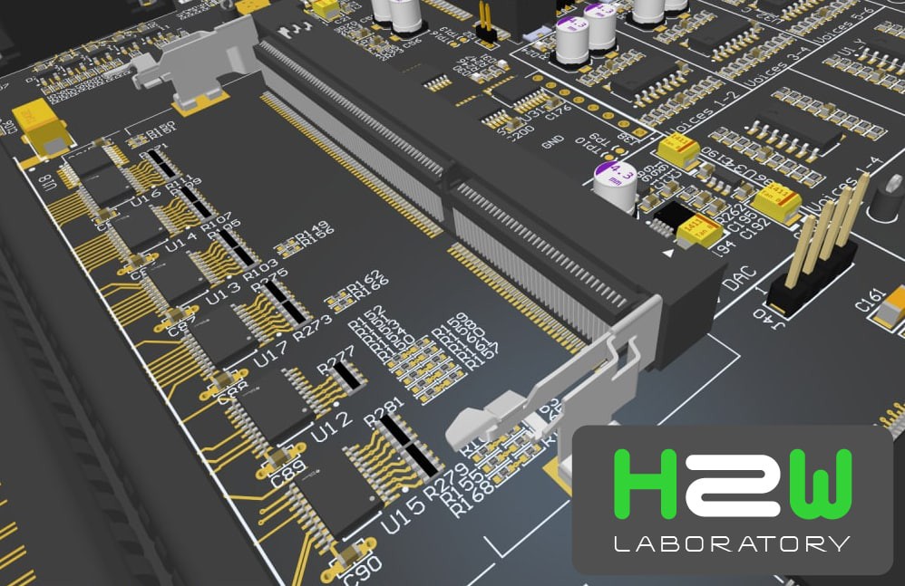
Using an off-the-shelf SODIM first of all saves development time. But it also gives a certain advantage in terms of the use of printed circuit board area, because components can be installed under the module.
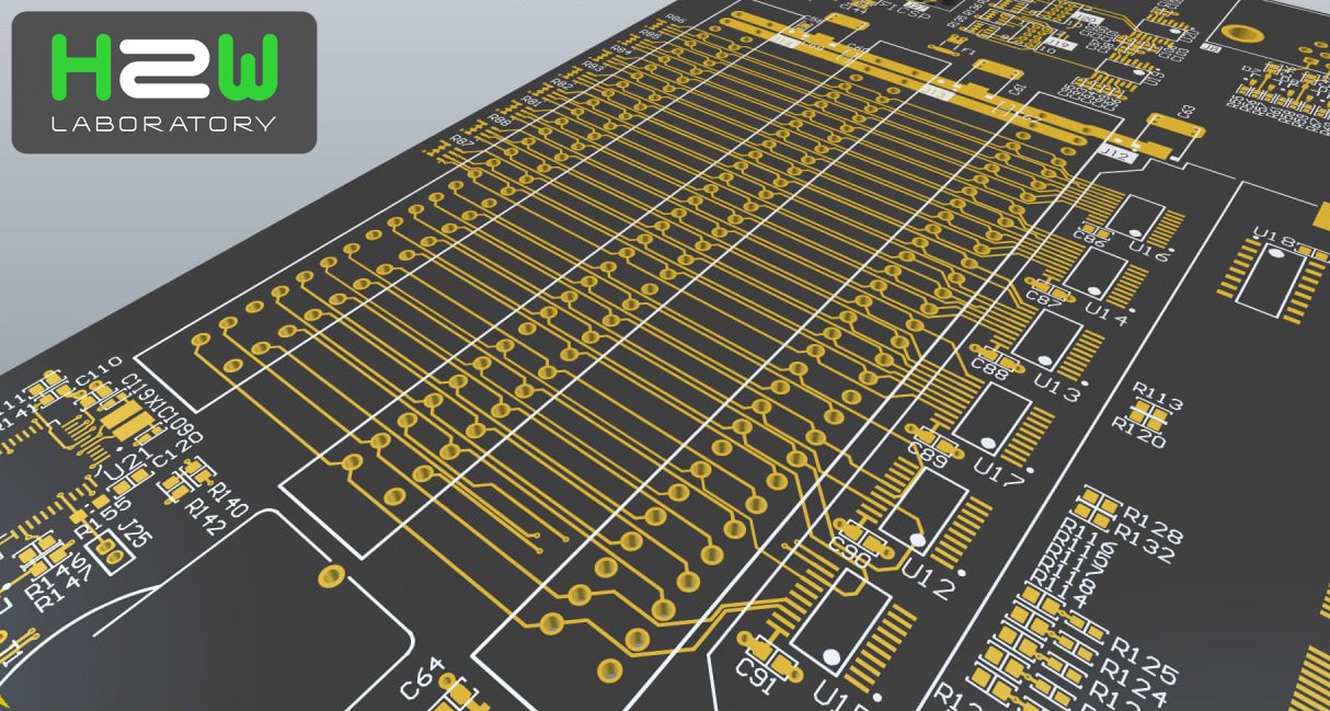
There are three slot slots of 64 pins each. On the far edge you can see the terminating resistors. The bus drivers are on the right side of the picture. The only thing I haven't decided is whether or not to do 5V compatibility. It doesn't make much sense since there is not a single board in the world for this slot. Other than that it is easier to build 3.3V logic today. On the other side of the scale is keeping hardware compatibility with the CPC6128.
 h2w
h2w