ElectronicABC
GERBER PCB:
https://mega.nz/file/6YYFBLqJ#wNYULXiXBTcZRSP9ZYLXIzb1CjjLXepdFCdey9F-bBs
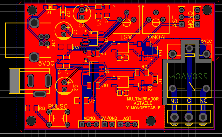
SCHEMATIC DIAGRAM
First we will start designing the schematic diagram with all its values of the electronic components and we take it to the tests to see how functional it is and after that we saw that it works perfectly so the schematic diagram is 100% reliable. It should be noted that this schematic diagram was made at EASYEDA.

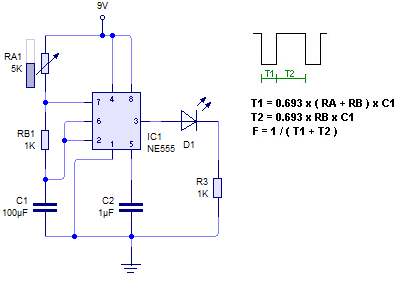
NE555 ASTABLE
When power is turned on, the capacitor is discharging and the 555 output goes high until the charging capacitor C1 reaches 2/3 of the supply voltage. When it reaches it the output of the 555 switches to zero and capacitor C1 begins to discharge through resistor RB. When the voltage across capacitor C1 reaches 1/3 of the supply, it starts charging again, and so on as long as the supply is maintained.
RA takes values between 1KΩ and 10MΩ, and RB always has to be less than RA
In this case, the high pulse and low pulse times are those that appear in the image
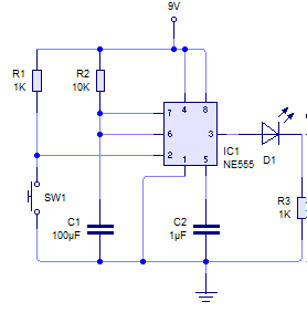
NE555 MONOESTABLE
By pressing the SW1 button, a small trigger voltage is applied to TRIGGER. This causes the output (pin 3) to go to the supply voltage VCC. The TRIGGER pin was originally loaded to VCC, and goes low to less than 1/3 of VCC.
When that happens, capacitor C1 begins to charge through resistor R1. When the voltage on this capacitor reaches 2/3 of the VCC voltage, the discharge pin 7 (DISCHARGE) is activated. At that time the output returns to 0 V.
FUNCTIONING
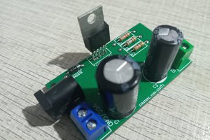
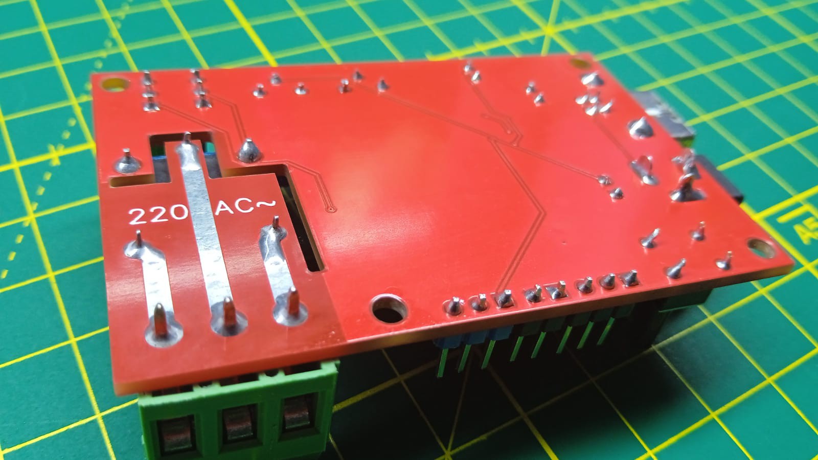
The operation of each multivibrator system is astable and monostable, we have already seen it before and now we will explain the operation of our PCB. We have 2 ne555 chips to make the two multivibrators. Initially we have 2 inputs at the voltage input, a type D computer connector to feed it directly from our computer since we have 5v at the output and another that would be from an external 5v source up to 5.5v has fast protection diodes against bad polarization also 3 outputs for each multivibrator a common one that is GND and 1 power stage output we can use both astable and monostable for our tests is configurable.
It should be noted that all components are SMD to reduce the size of the PCB
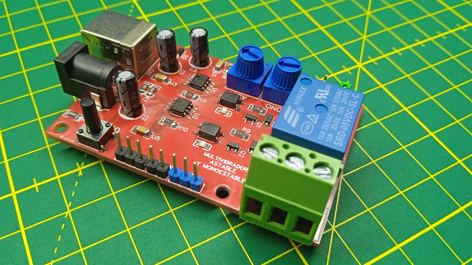
ELECTRONIC COMPONENTS
- 2 CI NE555 SMD
- 2 OPTOCOPLADOR SMD P127
- 2 TRANSISTORES SMD NPN 2N2222A
- 2 DIODOS 1N4148 SMD
- 2 DIODOS 1N5819 SMD
- 2 RESISTORS 1206 100 ohm
- 1 RESISTOR 1206 10K
- 2 RESISTOR 1206 150 ohm
- 2 RESISTOR 1206 220 ohm
- 1 RESISTOR 1206 4.7K
- 2 DIODO LED 0805
- 2 CAP 100NF 1206
- 2 POT 100K
- 1 BUTTON 4 PIN
- 1 CAP ELECTROLITO 1UF16V
- 2 CAP ELECTROLITO 100UF 16V
- 1 JACK DC
- 1 CONECTOR TYPE D
- 1 RELE 5VDC
- 1 BLOCK TERMINAL GREEN 3 PIN
- 1 ESPADINES
- 1 PCB
TECHNICAL CHARACTERISTICS
- VIN 5.5VDC
- 220VAC OUTPUT
- 3 DIGITAL OUTPUTS OF THE ASTABLE MULTIVIBRATOR
- 3 DIGITAL OUTPUTS OF THE MONOSTABLE MULTIVIBRATOR
- I MAX 120mA
EASYEDA
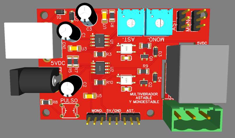
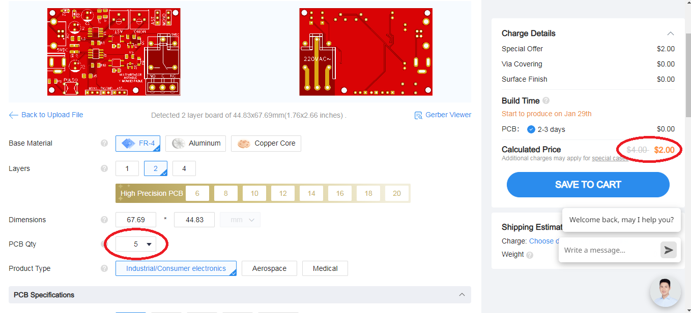
Once the project is finished with all the respective tests, we carry out the PCB design and we will obtain the routed tracks and the 3D image of how our finished PCB would look.
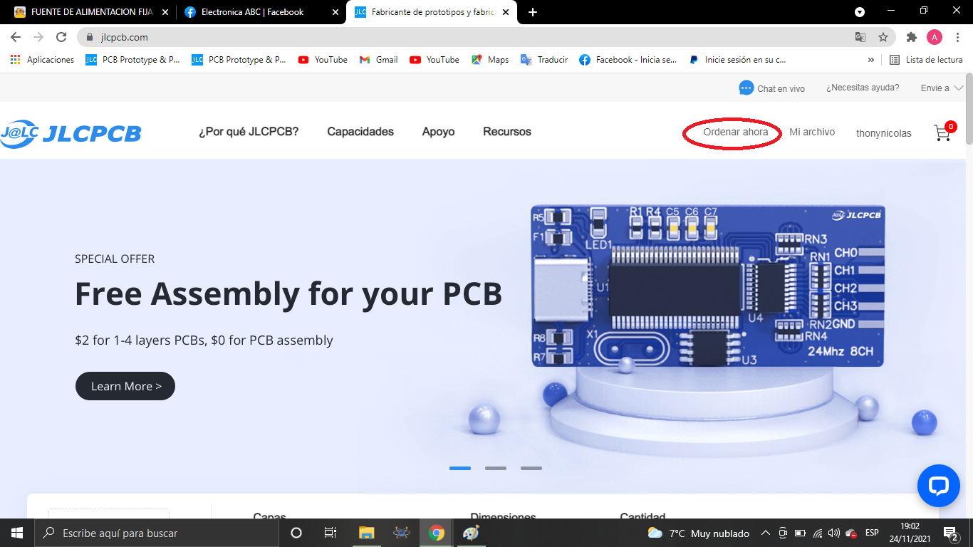
JLCPCB
Once the pcb is designed, we will send our friends from JLCPCB to manufacture our PCB.
5pcbs only $2
JLCPCB number 1 PCB manufacturing company worldwide professional pcbs and excellent finish.
GERBER PCB:
https://mega.nz/file/6YYFBLqJ#wNYULXiXBTcZRSP9ZYLXIzb1CjjLXepdFCdey9F-bBs
you can get your pcbs in different sizes and colors.
 w_k_fay
 Sagar 001
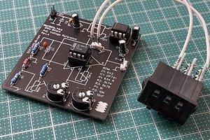
 555Techlab