Close
0%
0%

ArduGen

Low Cost Arduino Uno Arbitrary Waveform Generator.

Similar projects worth following
Arduino Arbitrary Waveform Generator using AD9102.

Currently on Software Design Phase
PCB's and schematics are completed and Hardware Release candidate 1 is ready

follow on twiter @EPetrongona , (https://twitter.com/EPetrongona) for live updates of the design.

Specifications (Beware most of them can and probably will be modified as the design progress)

Waveforms:
Sine-Cos
Triangle
Sawtooth-Ramp (Positive and Negative)
Square with variable Duty Cycle (0.5% resolution)
Noise
DC constant
Arbitrary Waveforms: 12 bit 4k Samples

AC specifications:
Min Frequency : 100 mHz (subject to change)
Max Frequency: 10 Mhz: (a experimental output may be available which can output unfiltered Signals of up to 80Mhz)
Sample ratio : 160 MSamples per second
Amplitude: 5Vpp

DC specifications:
DC Offset: +- 2.5VDC @ 5vpp
DC output: -5V to 5V

Misc:
Vertical Resolution: 2mVpp

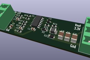
The idea behind this project is to create a low cost (~50 €) waveform generator, which is powered by an Arduino, for the hobbyists- students, who need to create basic signals, such as sine, pulse, ramp, but cannot afford to buy a proper WaveGen.

The Design process is based on the idea mentioned above and the following key points

  • ArduGen must be low cost. The target group consists of Students, hobbyists and fellow hackers who do not necessarily want to spend many $$ for equipment who may not use a lot.
  • Low cost does not mean low quality. The fact that the budget is quite limited does not mean that el cheapo components will be used. 2 € more expensive, may save everyone from endless headaches and frustration.
  • Small form Factor. Ideally i'll love to make it fit in an Arduino UNO compatible shield.
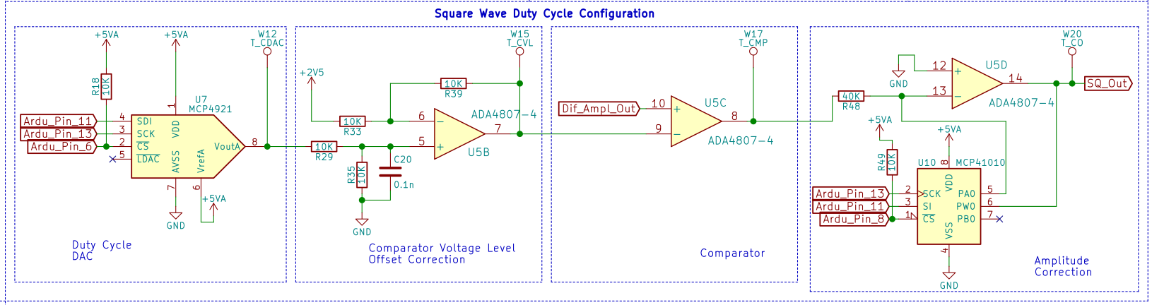
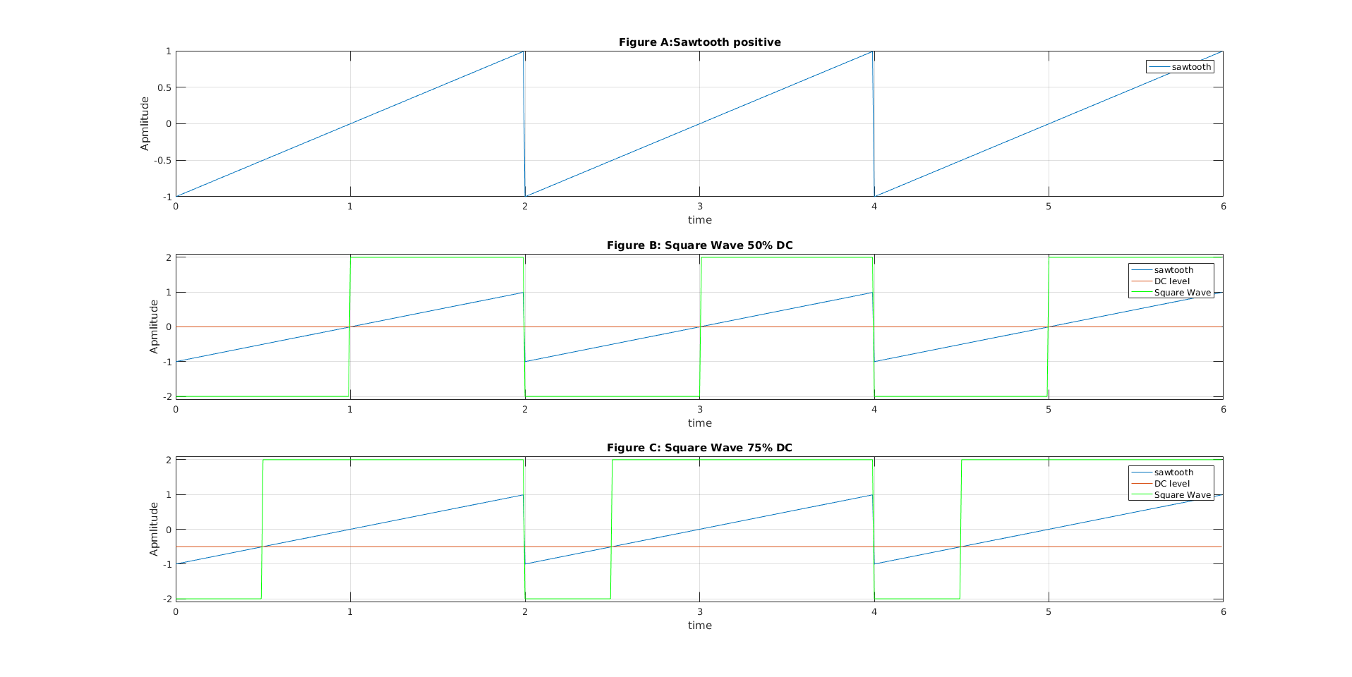
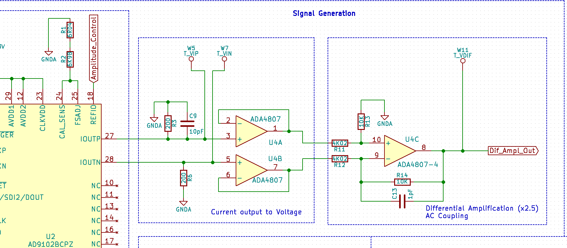
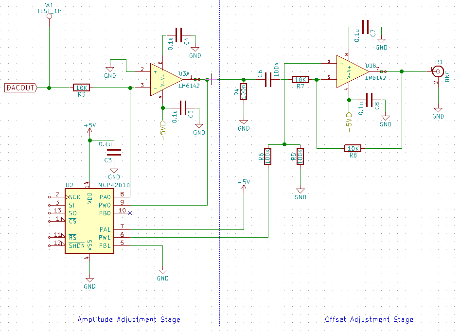
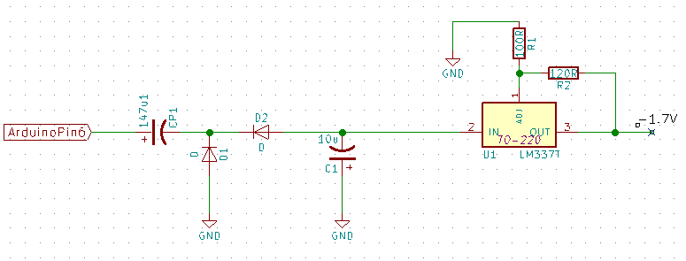
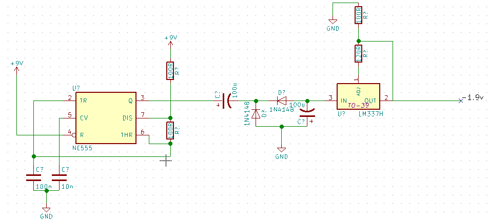
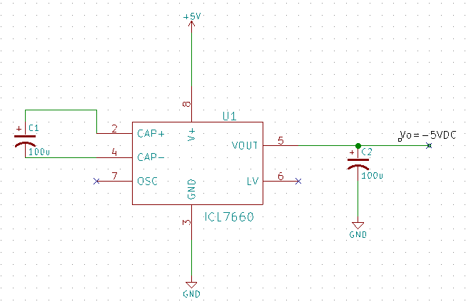
  • Negative Waveform Output. A very important aspect of the design is the ability to create waveforms that stretch into the negative axis. As a beginner myself, i know that working only with positive voltage, especially when using OpAmps, may be quite difficult some times. As a result this feature, despite the fact that it increases the overall cost a bit, and also makes the design a bit harder, is quite helpful to have.
  • Arduino UNO V3 is the brain of the circuit. That means that the UI, raw waveform values creation and pretty much everything else is done only by an Arduino. Maybe when the project is complete, a fork will be designed to make it function independently.
  • Open Source. Both the software and the Hardware are open source and licensed under CERN Open Hardware License v 1.2. for the Hardware and MIT Licence for the Software.That means that you are free to use, replicate, fork, pretty much do whatever you want, with the design. The only think i ask you to do, is to mention the original creator :)

Beware, although the Design is almost finished, the Specs can and will change as the project evolves. :)

Licensed under CERN Open Hardware Licence v 1.2 and MIT

http://www.ohwr.org/attachments/2390/cern_ohl_v_1_2.pdf

MIT_License.txt

Project Software License

plain - 0 bytes - 03/11/2017 at 22:42

Download

LICENSE.pdf

Project Hardware License

Adobe Portable Document Format - 95.73 kB - 12/28/2016 at 09:34

Preview
Download

  • 1 × Arduino Uno V3
  • 1 × AD9102 Data Converters / Digital to Analog Converters (DACs)
  • 2 × ADA4807-4 Op Amp
  • 1 × MCP4922 Data Converters / Digital to Analog Converters (DACs)
  • 1 × MCP4912 Data Converters / Digital to Analog Converters (DACs)

View all 9 components

  • DesBlog #5 Square Wave Duty Cycle Configuration

    Evangelos Petrongonas02/17/2017 at 16:29 0 comments

    Hello everybody and sorry for the absence, but it is exam period in the University so I didn’t have a lot of free time. First of all as you may have noticed in my twitter account the PCB is almost completed, and in the next week or so, the first prototype PCB’s, will be ordered :)

    Now let's get into this DesBlog’s topic, which is all about Square Waves and Duty Cycle. Square Waves with variable DC (DC=Duty Cycle), are very important signals in Electronics, as they can be used as clock signals, PWM modulation and many more. The main IC supports Square Wave Creation, using a comparator, which can function in two ways. It can either output the DAC MSB (if the MSB of the 14 bit DAC out value is 1 then it will output HIGH and if it is a zero it will output LOW), or the clock edge, which means that it will output a signal, which very much resembles the input clock. However, creating Square Waves this way is quite limiting, as its is complicated to adjust the frequency and almost impossible to change the Duty Cycle. A workaround for this is to load the appropriate pattern into the AD9102’s SRAM. This is not the optimal way to do it, though especially for such an important feature like the Square Wave Generation. For these reasons I have opted for a hardware implementation, which is shown down below.

    Well it might not be that obvious how it works in first glance, but it is pretty simple. First of all let's look at the basic concept. The IC’s DDS will generate a positive Sawtooth as shown in figure A. This signal is fed into an Op Amp which acts as a comparator. The other Input is DC Voltage level. When the input signal value is higher than the DC level, then the OpAmp output will jump to Positive Voltage saturation level, in this case +5V and when it is lower it will output -5 V, which is the negative Voltage Saturation value. So by changing the DC Voltage level, the Duty Cycle can be adjusted as shown in figures B and C. As far the frequency is concerned this can be configured by the sawtooth frequency. Bear in mind that the axes are arbitrary and do not correspond to a real vale

    The other Op Amps and IC’s are auxiliary and their function is the following. The input signal coming from the AD9102 is AC coupled which means there is no DC offset and the mean value is zero. In order for the comparator to work, the DC level must take both positive and negative values. This is done using a DAC (U7-MCP4921), in order to create a precise DC voltage in the range of 0-5Volts. Afterwards it is fed into the non inverting input of the OpAmp. The inverting input is a 2.5 Volt reference and the opAmp is in a unity gain Differential topology. This configuration is used also for the output offset generation so it will be covered in more detail in a future DesBlog, but for now just to give you an overview when the DAC output is 0 then the Voltage Level will be -2.5 V and when the output is 5Volts, the voltage level will be 2.5 V. This is the drawback mentioned in the previous DesBlog, caused by the Signal Generation Opamps.

    Last but not least the Amplitude must be configurable, as the comparator output will output a 10 Vpp signal. This is done with the help of an opAmp which is in simple Inverting configuration, but the feedback register is implemented using a digital potentiometer (U10-MCP41010) in order to set the wanted gain (which is less than one, as we want to decrease the Amplitude), just like we did back in DesBlog #1.

    That’s all for today’s DesBlog and as always I’ll be more than happy to hear your thoughts and suggestions.

    See you all next time :)

  • ​DesBlog #4 Signal Generation OpAmps

    Evangelos Petrongonas01/21/2017 at 10:13 0 comments

    elcome back everybody, the ArduGen Schematics are, hopefully, completed and most probably only minor tweaks will change in the design from now on. However, I do not want to publish a design which, will be scrapped eventually, so instead of releasing the schematics all at once, I’ll reveal it in small steps in each DesBlog.

    This time we’ll talk about the Signal Generation Op Amps. As you can see in the schematic below, this module consists of three Op Amps, the function of which, will be explained down below.

    For the time being, please ignore the Main IC which is an AD9102 Waveform Generator, as it is the heart of the design and requires a Log of its own. Before we proceed, though, the following must be mentioned. The AD9102 has a differential current driven output, and in its current configuration, it outputs a maximum current of 5 mA. (more details in a future DesBlog).

    The vast majority of Waveform Generators, output Voltage signals and this one is no exemption, so our first task is to transform the current output into a voltage output. This is done by using the 200 Ohm Resistors. As practically, no current flows into the OpAmp inputs, the Voltage across the resistors is 1 V for a current of 5 mA. IN order to ensure accuracy, the signal is buffered using two OpAmps in a voltage follower (buffer) configuration. The now buffered signal, is ready to be amplified. Both the positive and negative current signals (Beware negative doesn’t mean I<0, it means In= Imax-Ivalue), are fed into the non inverting and inverting inputs of the Amplifier, respectively, which is in Differential Amplification topology, with a transfer function of

    .The above equations is not exactly true as, i have not taken into account the Capacitor in parallel with Rf. However this may not be in the final design, and will be used only if the first tests show a high frequency noise. Even if it is used however, it will act as a Low-Pass active filter, with the same Amplification ratio as above. Moreover, due to the differential, amplification, the signal is AC coupled, as the common DC offset is removed, so there is no need for an external AC coupling Capacitor. This is mostly a good thing, but it has a downside, which will be made obvious in a future DesBlog.

    A question now arises, why the amplification is only 2.5 times instead of 5, as it is shown in the Specs (5Vpp Output). The answer to this question lies in the GBW vs Frequency Curve, a diagram of the maximum amplification of the OpAmp, in the various frequencies. Higher Frequency equals to lower Amplification ratio, so to avoid Amplification distortions, the amplification will happen in two stages.

    One last note, for those who have read the previous DesBlog, as you can see the OpAmp used now, is the ADA4807-4 a 4 channel IC, which is better than the LM6142, in almost every aspect, especially as far as the GBW and the SR are concerned, while maintaining very low power consumption.

    See you all in the next DesBlog, where we will take a look at the square wave, Duty Cycle and Pulse Generation Module :)

  • DesBlog #3 Changes,Changes and more Changes

    Evangelos Petrongonas01/09/2017 at 20:03 0 comments

    Hello everybody,

    Greetings from the snowy Athens :),

    I hope you' ve enjoyed the last 2 DesBlogs, because now, well......everything is changing.........

    Yes, it is not a joke, due to a fundamental change in the DAC IC, which required a different Analog Stage, ,the output stage must be redesigned.

    However, i have, hopefully, almost completed both the Analog and the Digital Design of the Circuit (Spoiler: some hints can be found at the components used in this project ;) ), so expect a new DesBlog, where we'll analyse the circuit step by step, really soon :)

    I apologize for the inconvenience, but that's the beauty of designing, you are always going to make changes and tweaks. Moreover i have decided that the next Blogs are going to be a bit more comprehensive and in depth, so they can act as a tutorial for the inexperienced hackers out there

    Thank you for your understanding and i'll see you soon very soon :)

  • DesBlog #2 Analog Stage

    Evangelos Petrongonas01/03/2017 at 12:51 0 comments

    Happy new Year Everybody, welcome to this 2nd DesBlog. Today we will talk about the Analog Stage, which is the Output Stage of our Wave Generator.

    Before we begin analysing the circuit let's take a look at the IC's we are going to use.

    1. OpAmps. Well... pretty much the most important decision for the Analog Part of the frequency is the OpAmps that will be used. They need to be
      • Rail to Rail I/O so that we can use most of the -limited- voltage selection that we have in our disposal.
      • Very Low Power. Do you remember the negative Power Supply that we designed last time. It had the limitation of low current output, it would drop to around -4.75 V, when drawing 5 mA of current . In order to avoid that issue, the supply output current should be kept to a minimum.
      • High Gain Bandwidth Product. GBP, usually specifies the maximum frequency that the OpAmp will retain it's unity Gain. If the max frequency is exceeded, then the Op Amp will output a smaller, in terms of Vpp, signal. To overcome that obstacle, a high GBP is required
      • Fast Slew Rate. SR is an indication of how quickly the output of the OpAmp can change and is measured in V/μs. A higher frequency signal, will transition faster from Voltage A to Voltage B and the Op Amp must follow the pace. If it lags behind the the Signal will be distorted. For the particular application an SR higher than 10 V/μs is sufficient.
      • Low Cost . As everything else in this project budget is an issue.

    And the winner is................

    LM6142 !!!! http://www.ti.com/product/LM6142

    LM6142 is a Dual Op Amp from TI which, pretty much fulfills most of our needs.

    it has a Rail to Rail output swing of +- 4.995 V, low supply current 650μΑ/ per amplifier, slew rate of 5-30 V/μs and Unity Gain around 5 Mhz. if you also consider that is relatively low cost it's a perfect IC.

    1. Digital Potentiometer. Not much to cover for the digital Pot. It will be used to determine the Amplitude and Offset of the output Signal. A 10k 8bit low cost Potentiometer is all that is needed. The reason that a digital pot is used instead of an analog one, is because the Amplitude and Offset adjustments will be done through software ooohhhhh.

    The ic that was selected is the MCP42010 from Microchip http://www.microchip.com/wwwproducts/en/MCP42010

    Beware though that in the future it might change from the 2 channel to 3 channel variant, depending on the Digital Stage Design.


    Now we are ready to discuss the circuit itself.

    And voila :

    Hopefully is not very complicated and the more experienced hackers out there will understand it in a blink of eye.

    The output DAC is feeded into the Inverting Input and the first Op Amp is in a simple Inverting Configuration. The output is ,where Po is the first channel of the Digital Potentiometer.

    Since the maximum Pot Resistance is 10K and R3 is also 10K the max gain of the opamp is 1. As a result the amplitude resolution is expected to be around 15-20 mVpp, depending on the Dac Output Voltage (More on that in the next DesBlog.)

    The signal however is dc biased, as the dac output is positive. In order to remove the dc bias, a coupling capacitor is connected in series with the next opamp. In addition a high value resistor is used, to avoid dc current block. The capacitor and the resistor combined is a Low- Pass Passive Filter. Now that the signal swings around Ground (0), a Dc offset can be easily implemented using one more opamp. Ideally it would be configured in a Voltage follower-buffer configuration, but the fact is,the input signal is inverted, and it would remain inverted. For this reason a Differential Amplification topology is used. The output ,according to the following equation, is :

    ,where V1 is the output of the previous OpAmps and V2 is the Voltage offset which is created by the second channel of the Digital Potentiometer which acts as a Voltage Divider. The above equation for the given resistor values equals to

    That way we can now configure both the Amplitude and the DC offset.

    One last note though,...

    Read more »

  • DesLog #1 ​Negative Power Supply Design

    Evangelos Petrongonas12/27/2016 at 20:03 0 comments

    Hello and welcome to the 1st Design Log or DesLog. Every now and then new logs will be uploaded, in order to keep you informed and suggest new ideas for the project.

    For this first DesLog we will take a look in the Design of the Negative Power Supply for the Output Operational Amplifier. This stage is quite crucial in order to determine the output specs of the Waveform Generator. The output current is limited in order to maintain -5V without too much deviation. After the first two unsuccessful attempts, a final design may, fingers crossed, be ready. The failed attempts are the following :

    1st Attempt:

    The Arduino was used in order to produce a 50 % DC pulse and then it was kind-of rectified so to create negative voltage, then signal was fed to an LM337T Negative Voltage Regulator. The problem was apparently that the the voltage after the rectification wasn't high enough and the regulator wasn't working. Moreover this method utilized the Arduino to create the oscillation (about 100KHz) required by the circuit to operate. As a result this design was abandoned. (The circuit described above is visible in the figure below)

    2nd Attempt:

    The natural way forward was to increase the voltage in the Rectification Circuit. In order to do so, instead of creating the oscillation from the Arduino, a simple NE555 timer IC was used to take its place. An extra benefit of that approach was that the Arduino code was no longer needed to produce the pulse, saving up valuable RAM space and processing time. This attempt though had, a huge downside, the fact that it required an external 9V Power supply, which was not in line with the project's main concept.

    3rd Attempt

    Back to the drawing board for take three. This time a specialized IC (ICL7066) was used to both invert the 5 V input and produce -5V, as well as regulate it. The IC uses the same method as described in Attempt 2, but with much higher power efficiency (~95%). Unfortunately that translates into slightly higher cost for the final product. Another disadvantage is the fact that the voltage is regulated for an output current of around 10 mA which is not as high as it was initially designed. That limitation however, is acceptable , as most Waveform Generators are used with HiZ loads (in this case more ta 1Kohm input impedance).


    Finally further testing will take place wth the MAX680 IC, which claims even better power efficiency, but it will have to wait for a future DesLog

    I hope you enjoyed this first DesLog and i'll be more than happy to see your thoughts and suggestions

    See you soon :)

  • Hi :)

    Evangelos Petrongonas12/27/2016 at 13:00 0 comments

    Merry Christmas or better happy Newton Day everybody.

    This is the first log of a new, actually my first, project called ArduGen.

    ArduGen is a short-of-an Arduino shield, capable of producing basic waveforms such as sine, pulse, ramp and more TBD. The heart of this project is a 12bit DAC, with 1 mV resolution, capable of producing accurate waveforms. Another feature of this project is the ability to create negative -YES Negative- waveforms, which is very handy for those who want to test OpAmps or, those into Audio Projects.

    Currently in very early Design Stage :)

    More to come SOON :) :)

View all 6 project logs

Enjoy this project?

Share

Discussions

bonapo3079 wrote 11/18/2022 at 16:02 point

<a href="https://bbalbaniavip.com/">Big Brother Vip 2 Albania</a> me te rejat nga edicioni 2 i big brother per kete sezone.


Shiko sezonin e pare te bbvip kosova live <a href="https://bbalbaniavip.com//">Big Brother Vip 2 Albania</a>

  Are you sure? yes | no

EmilHarvey wrote 08/22/2022 at 10:03 point

The Arduino can be used with no additional hardware. The only external circuitry required is an LED and some connecting wires. The Arduino provides an easy-to-use software development environment to write software for the Board. I need to read academized reviews now. The Arduino has built-in support for plugging in and out various types of sensors and actuators for handling inputs from switches, potentiometers, light sensors, thermistors and more!

  Are you sure? yes | no

xaver schrems wrote 03/24/2021 at 12:58 point

Hey Evangelos, great project, I love the idea! Seems like you lost trace of the project, because you last updated it in 2017. So I was courious if you could maybe post the schematic, so other people (including me) can continue your work on the project. I recently stumbled across the idea of building a cheap, simple but decent waveform generator too. Searching for an adequate dds chip, I also picked the AD9102 and then found your project. So I'd love to see your progress. Thanks in advance and greetings from Austria!

  Are you sure? yes | no

Similar Projects

Does this project spark your interest?

Become a member to follow this project and never miss any updates