This is the next iteration of my solar charger work. The last one, Solar Charger & Balancer, was intended to handle a string of PV panels in a mix of parallel & series configurations, and included a battery balancer. PVC follows the trend with residential inverters and is designed as a panel level charger that can handle up to 500W and dumps a regulated 56V onto a common rail that can be aggregated with other panels to charge a battery stack. It also incorporates the hardware MPP tracking design that was proved out in Solar Charger & Balancer.
I chose to stick with 56V because it is a relatively safe voltage and doesn't require insane currents to get to a few kilowatts. Sticking to moderate voltages also reduces design complexity, component stresses, and cost. Whereas Solar Charger & Balancer used a SEPIC converter, PVC is a dirt-simple, non-synchronous, non-isolated, flyback. There's no requirement to buck & boost the panel voltage since even the most efficient 500W monocyrstaline panels' MPP voltages are well below 56V. It is significantly smaller because of this.
PVC is intended to bolt directly to the back of the panel and connect to a common bus that charges the battery. With independent converters, some sort of controller is required to coordinate the chargers and protect the battery stack from being over charged. It is possible to include a charge algorithm in PVC's firmware, but it would be nice to have some centralized control to monitor the total charge in & out, health of the panels/chargers, etc. So, I have decided to use Power Line Communication (PLC) to communicate with the chargers. The PLC & controller will be added to the next design revision: this initial design only includes the converter core.
SPECS
Preliminary specifications of development board based on bench and limited field testing. With a Vin less than ~ 32V, the output power will be thermally limited. In reality, most PV panels with MPPs less than 35V are rated for 400W or less and will be the limiting factor.
- Vin: 25 - 40V DC
- Ain: 13.3 - 21.3A
- Vout: 56V
- Aout: 8.9A
- Pout: 500W
- Peak efficiency: 95.7%
- Average efficiency: 94%
- Topology: interleaved, non-isolated & non-synchronous flyback
- Switching frequency: 200kHz
- Control mode: peak current
- Controller: PIC16F1776
- MPP method: hardware tracking of Vin
- Cooling: natural convection via heatskink to case
- Operating temperature: -40 - +50C unverified
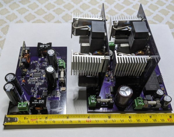
- PCB dimensions (LxWxH): 11.5x7.2x4cm (4.53x2.83x1.57")
THEORY OF OPERATION
The converter consists of two non-isolated flybacks running 180 degrees out of phase. This reduces peak currents in the plant and reduces input/output current & voltage ripple. Each phase employs an inner current mode control loop that manages the duty cycle with an outer common voltage loop. In theory, this ensures that the power output of both phases is equal. A low-side MOSFET and Schottky output diode form the plant switching pair, and each contain an RC snubber to control ringing.
Input & output voltage sensing is performed with resistive dividers that provides the sense signal for both the input & output voltage control loops. Current sensing is performed with a high-side sense resistor and an amplifier that provides the appropriate ramp signal for the current loop. Since the amplifier's bias positive supply is Vin, a level shifter (Q101, Q103) is required to ground reference the signal. R101/R108 & R113/R117 set the gain for each phase.
The Microchip PIC controller configures peripherals (Opamp, Comparators, timers COG, PWM, PRG) at boot so that the converters operate autonomously. With the exception of output over-volt protection, the PIC MCU functions as an administrative controller that provides an RS232 console interface and manages the startup configuration. Various operating parameters are stored in NVM including MPP tracking voltage, output voltage, current limit, etc.
A type 2 compensation network is used for the output voltage control loop: the error signal sets the starting voltage for the PRG (ramp) which provides slope compensation. A type 2 error amp is also used to track the MPP voltage. When Vin is above this loop's reference voltage it is essentially off. When Vin reaches the MPP reference, it engages by reducing the output error signal (via Q201) to maintain Vin at the MPP value. This effectively reduces the plant gain to match the converter's impedance to the PV panel. See hardware MPP tracking for a more complete explanation.
The converter's input consists of a simple LC filter and bulk capacitance to reduce current ripple and conducted EMI. At Vin low-line & full power, the converter's impedance will be lower than that of the input filter. However, this is mitigated by the MPP loop since it is not expected that a single panel can supply more than 350W below 30 volts. Vout consists of a similar arrangement with bulk capacitance and an LC filter. The output is also fused to protect the battery stack and other external components against a short failure within the converter.
The main bias supply is provided by a daughter-board utilizing the TI LM5161 buck controller. The converter is energized above ~ 19 volts and provides a regulated 12V for the gate drivers and a 5V LDO for the controller. A separate floating bias supply is required for the current sense amplifier: zener D101 and R106 form a simple dissipative supply referenced to Vin for both phases.
DESIGN IMPROVEMENTS
The design needs some revisions: some are dimensional or layout for improved thermal performance, but I won't go into those here. If you do decide to build this version, beware that the micro-USB connector pinout is reversed: I used a horizontal mount as a reference when making the footprint and failed to validate the pin mapping.
Current sense method. Current sense transformers are my preferred choice because of their simplicity, excellent signal to noise ratio, and inherent isolation. I was curious how well an active sense & level shift would work, and this design afforded the opportunity. It works reasonably well, but there is some duty cycle jitter at light loads (<200mA) because of some leading edge ring at the start of the period.
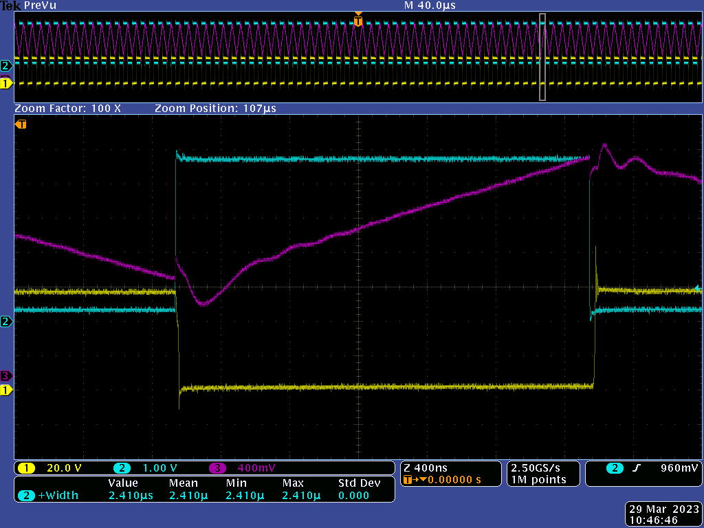
This is a trace near full power, but the leading edge ring is clearly visible, and is over-shoot from the opamp. A small capacitor (~15pF) across the inverting input to output may reduce this.
Floating bias supply for current sense. While the zener shunt functions well to provide the floating bias supply for the opamp, I failed to account for the required zener knee current (I_zk) when first energized. Hence, the current amplifiers (U103/5) don't come online until ~ 28V. As a work around I changed R107/116 to 3K to limit current thru the PIC ESD diodes since the level shift transistors (Q101/3) are biased and dump Vin on the sense pins. I also reduced R106 to 3K to increase the bias current. In the revised design I will likely revert to a CT since less circuitry is required.
LDO blocking diode. The 5V LDO, U101, should have a blocking diode on its DCIN+ pin to prevent power from the USB console connection back-feeding Vin. This occurs because the LDO uses a FET pass element.
HW based over-volt shutdown. I avoid relying on firmware for plant & safety control, but since this was for development only I didn't incorporate a hardware over-volt shutdown (I think I ran out of comparators that could map to the Vout sense pin).
Poor regulation of Vout at light loads and high Vin. Because this is a non-isolated flyback, Vout will drift up even with the control loop pulse skipping. It doesn't take much load (~20mA) to prevent this, and a burden resistor would certainly work: but this is > 1W of dissipation. Other solutions include leveraging the over-volt protection with auto-restart control in firmware. Alternately, one phase could be shutdown. In practice, this may not be a concern since the intended application is a charger that will be turned off when the batteries are full.
Add a relay to output. Another problem with non-isolated flybacks is that Vin appears on Vout when the converter is off, and current will flow limited only by the impedance of whatever's connected to the output. In normal operation this should not happen since the battery stack's voltage should always be higher than the panel, but what about a short on the output: the converter will shutdown, but current will continue to flow. The fuse may not offer protection since the panel's short circuit current (I_sc) may be less. A normally open SSR solves this problem.
Minaturize the bias power supply. I used what I had laying around since this board was for development, but the revised design will place the regulator directly on the main board. Whereas this one uses the TI LM5161 and a hand-built inductor, the on-board version will use the LM5017 running at 500kHz with an off-the-shelf inductor and take about 1/3 the space.