 macafeeje
Obligatory danger warning; there are several high potentials within an oscilloscope which you should become familiar with before opening any such device. Proceed with caution.
Original Fault Finding;
The list of faults when I first received my particular PM3310 was extensive. Most obviously there was no trace, only a single dot. I did not get round to investigating this fault immediately, as the scope would not pass it's boot check and it seemed logical to pursue this particular issue before looking at anything else. Once the scope was repaired to the point of passing a boot check, the lack of any X deflection became my next task.
I will limit my notes on the repairs to the board A20, the final amplifier, and in case it's useful...
- PCB under V2023 found to be discoloured with heat, tested to be defective. (V2007, 2016 and 2032 replaced as a precaution)
- V2038 tested to be defective
- D2023 (oq0017) signal in from D2021 found to be good, no signal at the output, suspect D2023
The scope was tested after replacing the defective transistors, however there remained no trace to be had.
It is not known whether the chip (D2023 - oq0017) failed first, causing the transistor to overheat and fail, or if the failed transistors (current source above pins 12/13 and/or constant current source at pin 9) ultimately lead to the demise of our X amplifier chip. From my research there have been a few X amplifier chips failed on this model scope, and whilst I could not speak to their exact means of failure, it does appear to be a common fault.
Other faults on A20;
- R2081 insulation broken, "sparking" from +125 to GND or +12 nearby traces (occurred after the above fault finding).
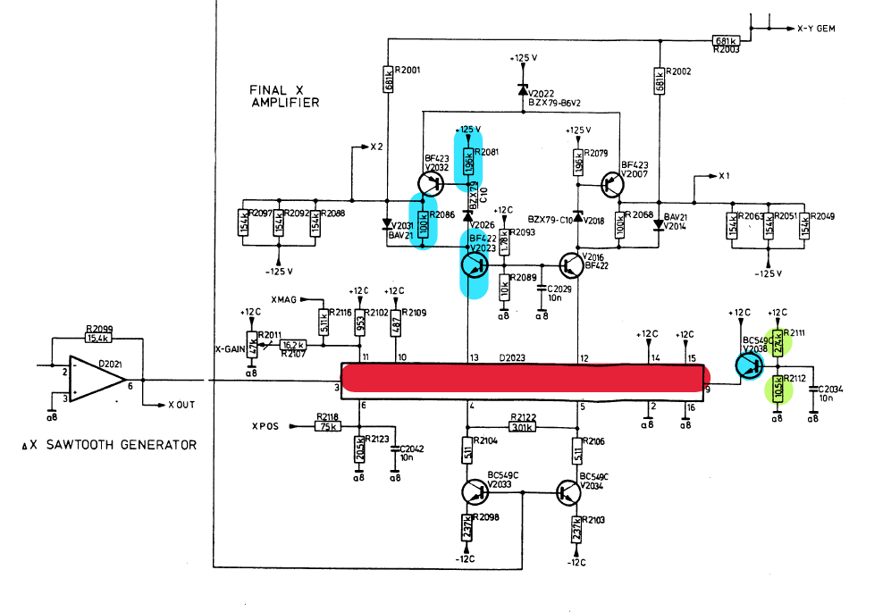
This excerpt from the PM3310 service manual (edited for context) shows the final X amplifier arrangement. A ramp signal is generated and buffered by the op-amp D2021 before the chip on pin 3. The X POS line to pin 6 is the left/right position of the trace, as controlled by the X POSITION dial on the front bezel. The gain is controlled as a product of X-GAIN, x1 gain adjustment, and X MAG, the x2.5 magnification dial. Pin 9 is a constant current source for internal chip functions.
Whilst the engineers creating the service manual left out the inner workings of oq0017, some though was given to its layout as pictured here. There is something to be inferred by the above and below symmetries from pin 13 to pin 4 and from pin 12 to pin 5. It could be reasonably assumed that a differential current between these two pairs would cause the X1 and X2 plate deflection voltages to vary, guiding the CRT trace from left to right with the ramp signal.

Early Attempt;
I include my earliest attempt at restoring an X trace here, as it is very simple to implement and could be done easily with a few minor components. The x2.5 magnification function will be lost.
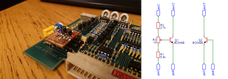
I was not at all familiar with the pure "analogue magic" that was to come, and so as I started my research into a solution regarding the peculiarities of a variable gain difference amplifier I of course came across the long tailed differential pair. The current source and sink above and below pins 12/13 and 4/5 seemed to fit with this topology.
Q1 and Q2 form the differential pair, that is the difference between the X ramp signal and the left to right position as set on the front X POSITION control. Ideally both transistors should be matched, and to reduce the effects of thermal drift, both should be thermally bonded to each other (most simply with the use of a zip-tie).
R1, 2 & 3 form a potential divider as a crude method of reducing the gain of the ramp signal. To set the trace width, R3 allows for a trimmable final gain.
The PM3207;
I stuck with the above arrangement whilst repairing the seemingly increasing number of faults with my scope. Later, I did find a repair log by (I think) Markus Dropmann in 2016 (google "Reparaturbericht digitales Speicher-Oszilloskop Philips PM3311"...
Read more »
 sjm4306
 kamalkedin123
 Ghani Lawal
 Christoph Tack