0%
0%
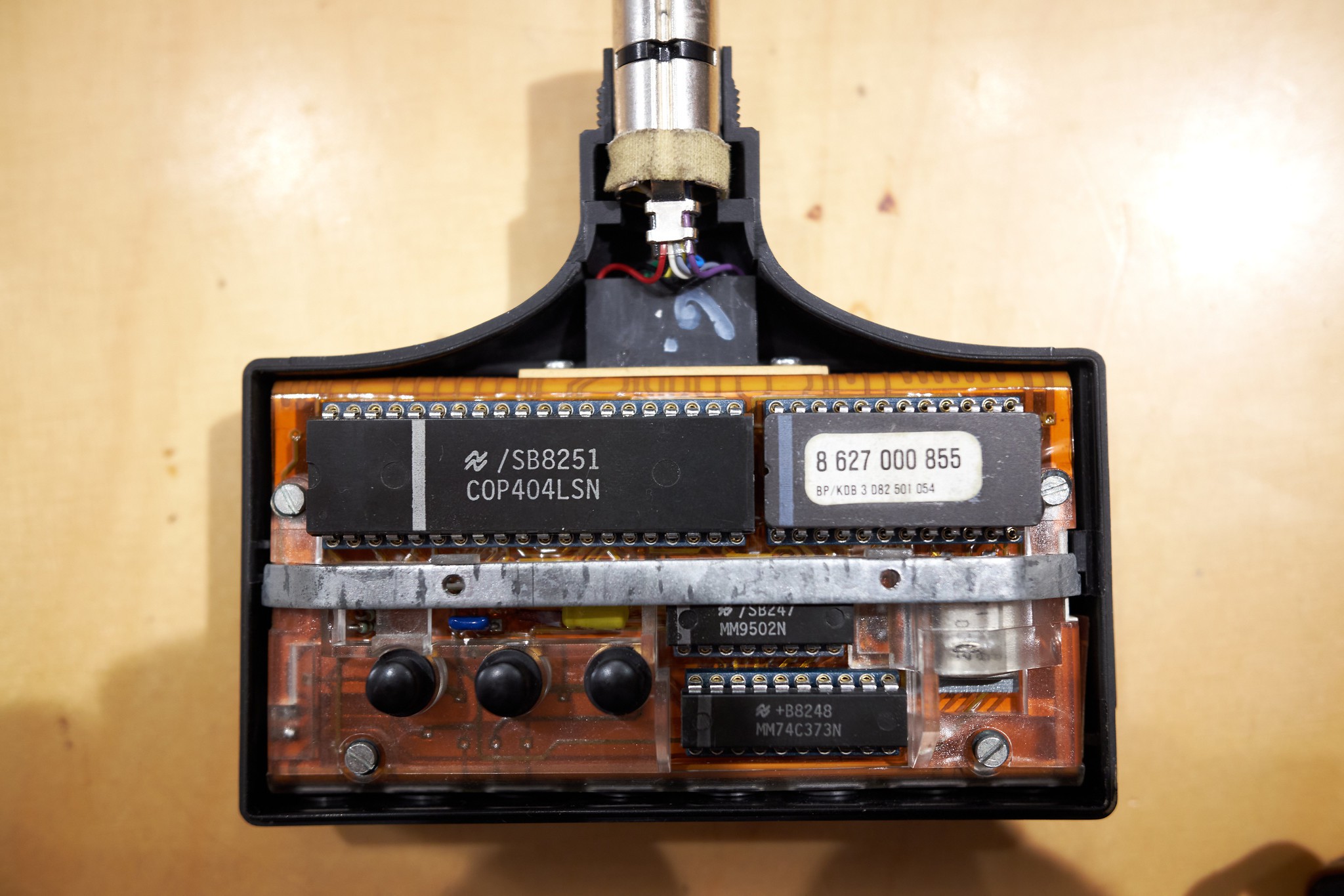
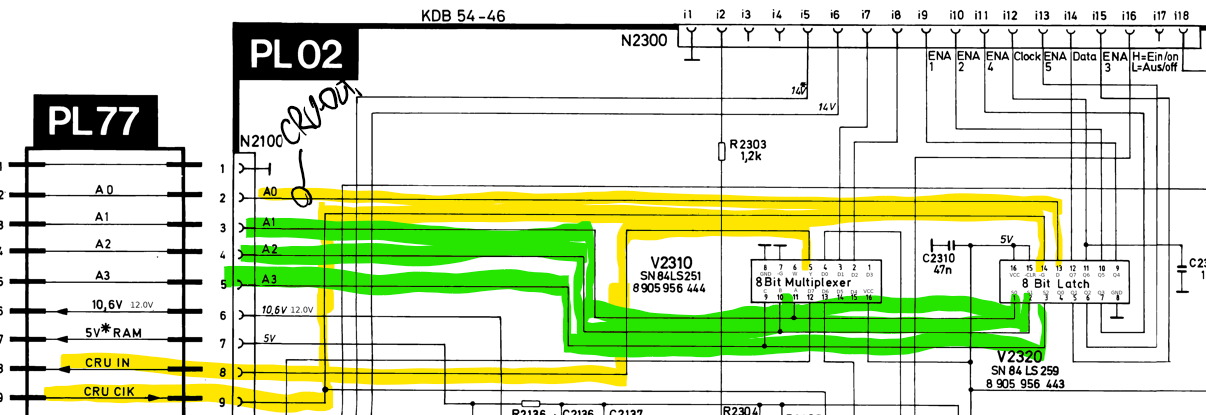
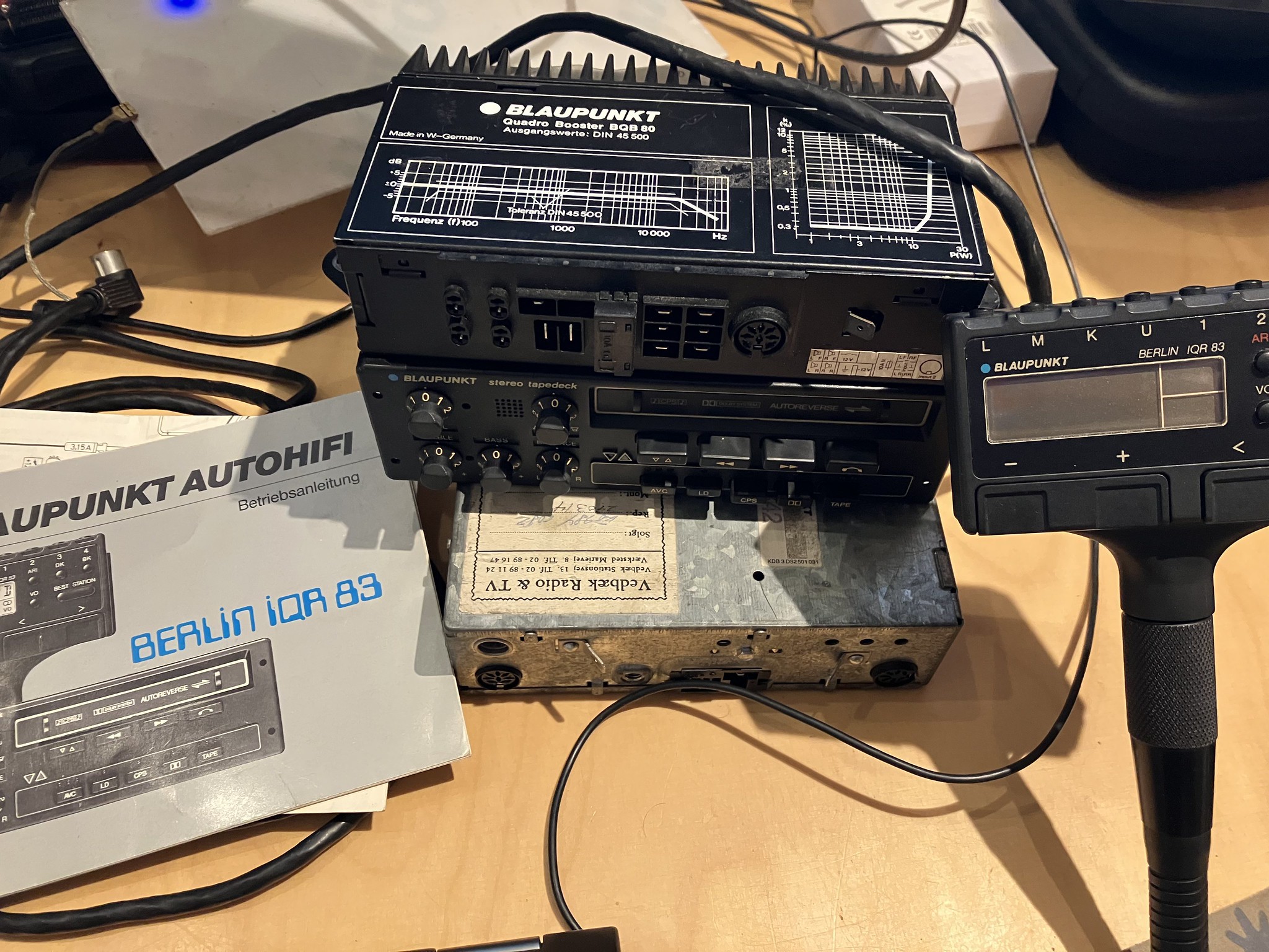
New life to the Blaupunkt Berlin IQR 83
"The worlds most expensive car radio"
"Der Autoradio das Denkt! Und sagt, was es denke!"
 Anders Dinsen
Become a Hackaday.io member
Already have an account? Log in.
Just one more thing
To make the experience fit your profile, pick a username and tell us what interests you.
Pick an awesome username
hackaday.io/
Your profile's URL: hackaday.io/username. Max 25 alphanumeric characters.
Pick a few interests
Projects that share your interests
People that share your interests

 Boxerbomb
 Артём Шакиров
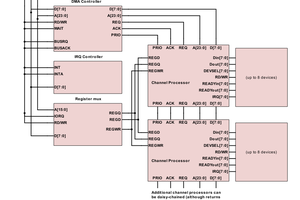
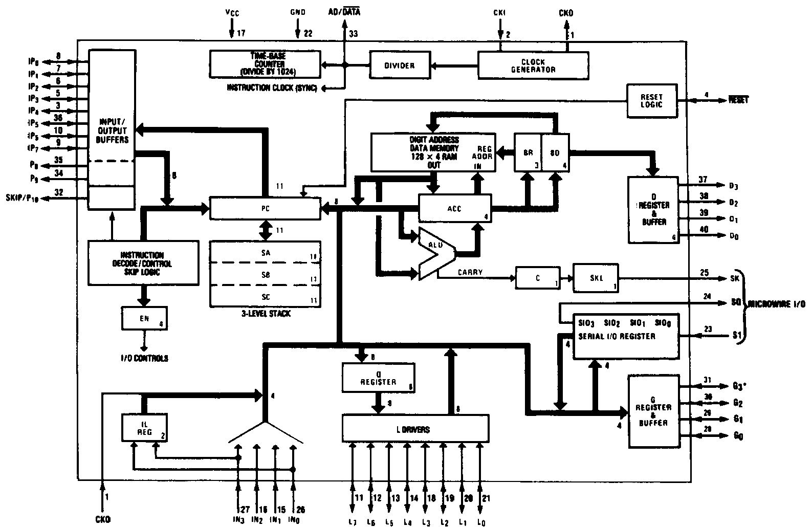
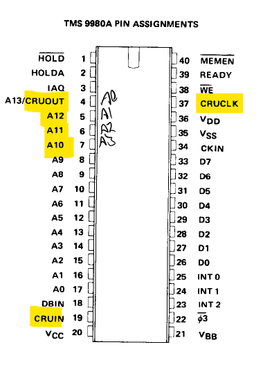
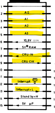
Thanks for the writeups of the TMS9900 and COPS400 microcontrollers. I saw ads for and read articles about them in industry magazines back in the day, but never encountered them in real-life. So it's interesting to learn about them decades on. 👍