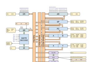
My current plan is to separate the system into the following logical blocks:
- A DMA controller, interfacing to the system and controlling access to the bus in order to allow the processor to load data from or store data into memory. The precise details of this will vary according to the host processor, so I may design multiple versions of this block (although to start with I will be aiming for Z80 systems).
- An interrupt controller. This allows the processor to send interrupts to the host computer when tasks have finished or otherwise need attention. Again, this will be closely coupled to the type of processor, so I may end up producing some variations on this design.
- A register multiplexer. This sits on the processor bus and allows the host computer to inspect or modify processor control registers.
- A daisy-chainable processor block, which can handle 16 data channels, each of which may (optionally) be attached to one input stream and one output stream (where a stream is either a DMA block or a port on a connected device) and has a local IO bus onto which up to 8 individually addressable devices may be attached. The processor will forward DMA/IRQ requests from processors further down the chain. Realistically, 2 of these blocks would handle the IO requirements of most plausible small computer systems, and adding a third would make a system that could handle just about any foreseeable requirement (of a single user PC, at least). For example the following setup would require 10 channels, and would therefore leave 6 available channels of a two-block configuration:
- keyboard in
- mouse in
- 2 UARTs (each requiring one input and one output channel)
- parallel out
- disk in/out
- video out
The processor itself will be design to be as simple as possible. I'm currently considering using 4-bit opcodes for common operations, with a few escape sequences to allow for up to 61 total operations. With either 2 or 3 registers, this should be enough to support moderately complex programs. Microcoded to reduce complexity. Probably a pair of 74181s for the ALU.
The most complex part will be the fact that each of the 16 channels needs to have the appearance of having its own processor. My original design had a lot of registers -- it would have had somewhere around 12 74AS870s (although those are very hard to get hold of at a reasonable price, and I'd need 8 times as many of the next logical contender, the 74*670, which is clearly infeasible). I'm currently revising my design to use some fast static RAM chips for registers; these will run at double the clock rate of the processor in order to allow both a read and write cycle per processor cycle. As I'm aiming to use authentic components that were available circa 1982 - 1983, I'm thinking of the TMS2149 (which was first available at the end of 1981 for ~$9 per chip, 1K x 4, 35ns), probably with a total of 4 chips (allowing access to 2 8-bit registers or 1 12-bit register per cycle). Allowing for control logic and latching in addition to the 35ns access time of the RAM chips, this will likely limit maximum clock rate to ~12MHz.
An initial version of the design will be implemented for performance testing and tweaking in an FPGA. As well as being easier to tweak and smaller than the final period-correct design, this will also run faster; I intend to use it in a system alongside a 20MHz Z80, and am planning on having it run at the same clock rate as the host processor. But that's another project that I haven't yet uploaded any information about....
For the final design, I intend to only use components that would have been available at a reasonable cost circa 1982-1983. But I'm also planning on minimizing board size as far as possible. I want this system to have been a realistic component to install in a high-end home computer. This means a lot of logic will be in PALs or GALs, probably...
Read more »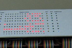
 Pavel
Pavel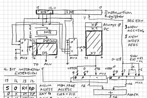
 zpekic
 2-Zons