 tomcircuit
rcl57mcu
This project came about because I stumbled across a TI-57 calculator with a "bad brain". The TMC1501 calculator-on-a-chip was faulty. This, in turn, led me to read more about this particular calculator and how the CPU inside functions.
Fortunately, I am 'standing on the shoulders of giants' here - three people that have been of great help to me are Joerg Woerner, Jeff Parsons and Paul Novaes. All humored me by answering my emails and helping me understand how the hardware works.
Joerg's DATAMATH pages are found here, and in particular contain a great summary of the TMC1501 IC that is the calculator-on-a-chip used in the TI-57.
http://www.datamath.org/Chips/TMC1500.htm
@Jeff Parsons TI-57 pages are found here, and extremely helpful is his collection of original Texas Instruments patents filed around the introduction of this calculator:
https://www.pcjs.org/machines/ti/ti57/patents/
Both Jeff and Paul have created TI-57 emulators. Paul's is an iOS app, and Jeff's is browser-based. Both emulate the TMC1501 CPU innards, which in turn execute the original TI-57 ROM code. So it is a faithful 'emulation' of the calculator.
Paul @n3times was kind enough to put his iOS app code up on GitHub:
https://github.com/n3times/rcl57
The 'guts' of the TMC1500 emulation are all contained within the 'engine' folder, and written in very generic and portable C. I learned an awful lot from studying this code.
The Quest
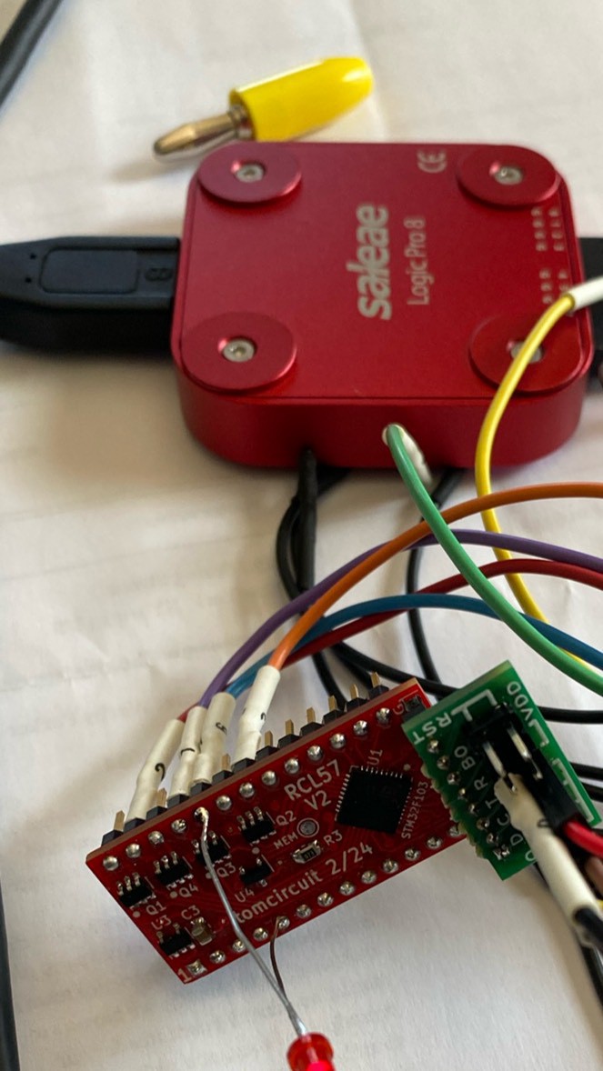
I began to hatch a scheme - could I put a modern microcontroller (MCU) to the task of emulating the 1970's TMC1501? Could this hardware emulator be then installed into my defunct TI-57 to make it live again, perhaps even better than before?


 Ted Yapo
 Stephen Holdaway
 Ben Patterson
 Jeremy Gilbert
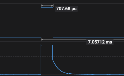
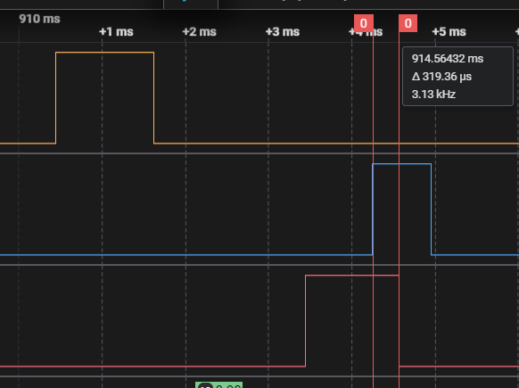
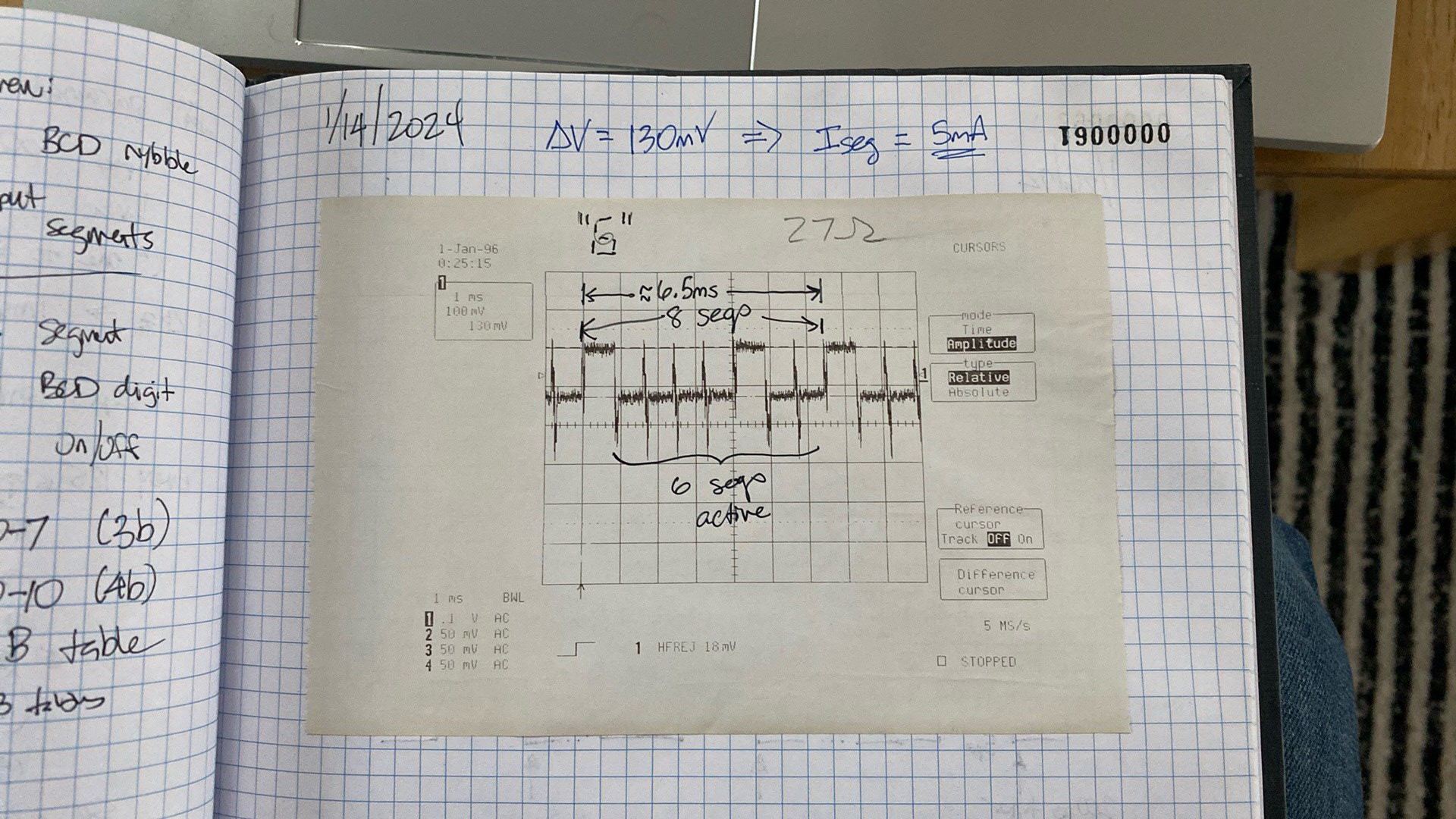
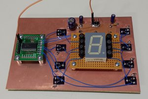
This looks good!