The MCU is a MSP430G2231 which is extremely small and limited but it comes in a PDIP package and is easy to program (see my last project). It is well suited for this application because I only need 1 shift register, 1 output pin, and a 1 MHz clock is more than sufficient. Additionally, it operates at a low Vcc voltage < 3.3V which comes in handy if I want plug the final signal right into Line In.
For the pink noise filter, I considered the designs from the SyntherJack blog and decided to go for a passive design like in Thomas Henry's circuit. I initially wanted to add an LFO and VCA to the front like in Jack's Ocean Noise Generator but after testing it sounded kind of weird on its own so I scrapped it. My main goal from this project was to learn how the values for the shelf filters were chosen so I decided to derive the equations for them by hand.
Digital White Noise Generation
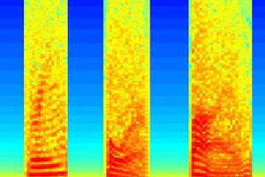
An LFSR is a shift register where some combination of higher bits are XORed together and pushed into the front of the register. It can be used to generate random numbers, or if it is polled fast enough it can create white noise. I found this website that lists a bunch of possible combinations that loop through all the possible combinations of bits. Since the MSP430 is a 16 bit MCU, initially I tried the 15 bit loop where you XOR the first and 15th bit and push that to the front. However, this had a really short cycle length and I could clearly hear the sequence repeating. I implemented a 32 bit version using two 16-bit registers in assembly, and for this sample code I'm using the 3rd bit and 21th bit (bit 2 and bit 20) ( 20 mod 16 is 4 therefore in practice I actually test bit 4 of the higher register).
I used the MSP430G2231 running at 1MHz and outputting to port P1 (couldn't be bothered to add the extra instructions to just output to one pin!)
while(1) {
    // R10 and R11 together form the 32 bit register
    // Carry flag (C) is the least-significant bit of the status register (SR)
    asm("   BIT #2h, R10"); // C <- R10 AND 0b00000010 (bit 2)
    asm("   MOV SR, R12");  // R12 <- C
    asm("   BIT #10h, R11");// C <- R10 AND 0b00010000 (bit 4 aka bit 20 of 32 bit value)
    asm("   XOR SR, R12");  // R12 = R12 XOR C
    asm("   RRC R12");      // C <- bit 0 of R12
    asm("   RLC R10");      // Rotate left through C
    asm("   RLC R11");      // Rotate left through
    asm("   MOV.B R10, P1OUT"); // copy R10 to P1OUT. P1OUT is configure so only P1.0 is an output.}
Analyzing One Stage
Before that, though, I looked at the circuit analytically and tried derive the gain at DC and high AC values.

If the input signal is DC, then C1 becomes an open circuit and no current flows through it. Therefore the output voltage is equal to the input voltage. If the input is high-frequency AC, then C1 becomes a short circuit (replace with a wire) and the output voltage is determined by the voltage divider created by R1 and R2:
Where A is the gain which is equal to the output voltage divided by the input voltage.
The next stages are mostly the same, but now you need to consider the effect of the previous stages (can use Norton's, etc). Overall, its possible to completely calculate this circuit with just the previously stated assumptions and calculating one stage at a time. Additionally, I didn't realize this in the beginning but you should also include the output resistor in your calculations. Since the output is not buffered, it will load the circuit and change the frequency response. I measured the input impedance (crudely) of my Line In jack to my PC and got a value around 24-32k, which pretty much aligns with Wikipedia's quoted theoretical 10k.
I did a bunch more math for the resistors...
Read more »
 Yann Guidon / YGDES
 Bruce Land
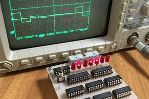
 Mitsuru Yamada