Close
0%
0%

Full-Adder Using 74LS283N

Binary adders: HalfAdder adds 2-bit binaries; Full Adder adds carry and 2-bit binaries. Multiple bits by cascading FullAdders. Uses 74LS283N

Similar projects worth following
57 views
0 followers
Here’s a brief overview of binary adders. There are two main types: Half Adders and Full Adders. A Half Adder can add two 2-bit binary numbers but cannot include a carry bit. In contrast, a Full Adder can add two binary numbers along with a carry bit. By cascading Full Adder circuits, we can add multiple-bit binary numbers. The IC 74LS283N is commonly used to demonstrate Full Adder circuits in practice.

Difference Between Half Adder and Full Adder

Before diving into the details of the full adder, let's compare the main differences between the half adder and the full adder.

A half adder has two inputs (A and B), which are both 1-bit binary numbers. It adds these two binary digits and produces two outputs: Sum (S) and Carry (C). The half adder is a simpler design but does not consider any carry bit from a previous addition, limiting its functionality. It is often used as a building block for full adders.

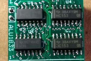
In contrast, a full adder has three inputs: two 1-bit binary numbers (A and B) and an additional carry-in bit (Cin). It adds these three inputs and produces two outputs: Sum (S) and Carry-out (Cout). The full adder is more complex as it includes the carry from the previous addition, making it suitable for multi-bit addition and applications in digital processors. The IC 74LS283N is commonly used to demonstrate full adder circuits in practice.


Full Adder Circuit Explanation: 

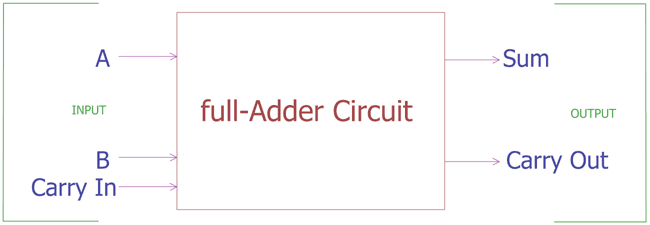
The Half Adder circuit has a drawback: it cannot accept a carry-in bit for addition. In contrast, the Full Adder can accept three inputs: A, B, and Carry In, producing SUM and Carry Out outputs. The equation is A + B + Carry In = SUM and Carry Out. The Full Adder Block Diagram shows it accepts three inputs, including a carry-in, and provides two outputs: SUM and Carry Out. By combining two Half Adders and an OR gate, we create a Full Adder circuit.

To understand the Full Adder in greater detail, including its construction using Half Adders, NAND gates, NOR gates, cascading adder circuits, and Tinkercad Stimulations, you can refer to our comprehensive article, Full Adder Circuit and its Construction. For additional insights and detailed explanations, feel free to visit our website.

  • 2 × 4pin dip switches
  • 4 × Red LED
  • 1 × Green LED
  • 8 × 4.7k resistor
  • 1 × 74LS283N Logic ICs / Arithmetic and Parity Functions

View all 9 components

  • 1
    Circuit Diagram

    I have included the circuit diagram above for you to follow. Next, Let us look at the explanation.

  • 2
    Pin Configuration and Circuit Explanation

    In this circuit, the pin configuration is as follows:

    • Pin 16: VCC
    • Pin 8: Ground
    • Pin 5, 3, 14, 12: First 4 bits (P), where Pin 5 is the MSB and Pin 12 is the LSB.
    • Pin 6, 2, 15, 11: Second 4 bits (Q), where Pin 6 is the MSB and Pin 11 is the LSB.
    • Pin 4, 1, 13, 10: SUM output, where Pin 4 is the MSB and Pin 10 is the LSB (when there is no carry-out).
    • Pin 9: Carry-out.
  • 3
    Resistor and LED Setup

    4.7k resistors are connected to all input pins to ensure a logic 0 state when the DIP switch is in the OFF position. This setup allows easy switching between logic 1 (binary bit 1) and logic 0 (binary bit 0). The circuit is powered by a 5V supply.

    When the DIP switches are turned ON, the input pins are shorted with 5V. Red LEDs are used to indicate the SUM bits, and a green LED represents the carry-out bit.

    This configuration allows for clear and straightforward monitoring of the binary addition process, with visual indications of both the SUM and carry-out results.

View all 4 instructions

Enjoy this project?

Share

Discussions

Similar Projects

Does this project spark your interest?

Become a member to follow this project and never miss any updates