 Mitsuru Yamada
1. Overview
Figure 1 shows the appearance of this Digital Sampler and Table 1 shows the specifications. This device is the origin of my Homemade Successive Approximation Register ADC project (2021). The aluminum plates on the top and sides of the enclosure have been removed. The external dimensions without knobs and other protrusions are 150 mm x 200 mm x 265 mm. The analog oscilloscope on the right side shows the sampled waveforms. I recently posted a video of the internal configuration of this device on YouTube. And it was featured on Hackaday's top page blog. This article presents a video of the actual operation of this device and explains its internal circuitry.
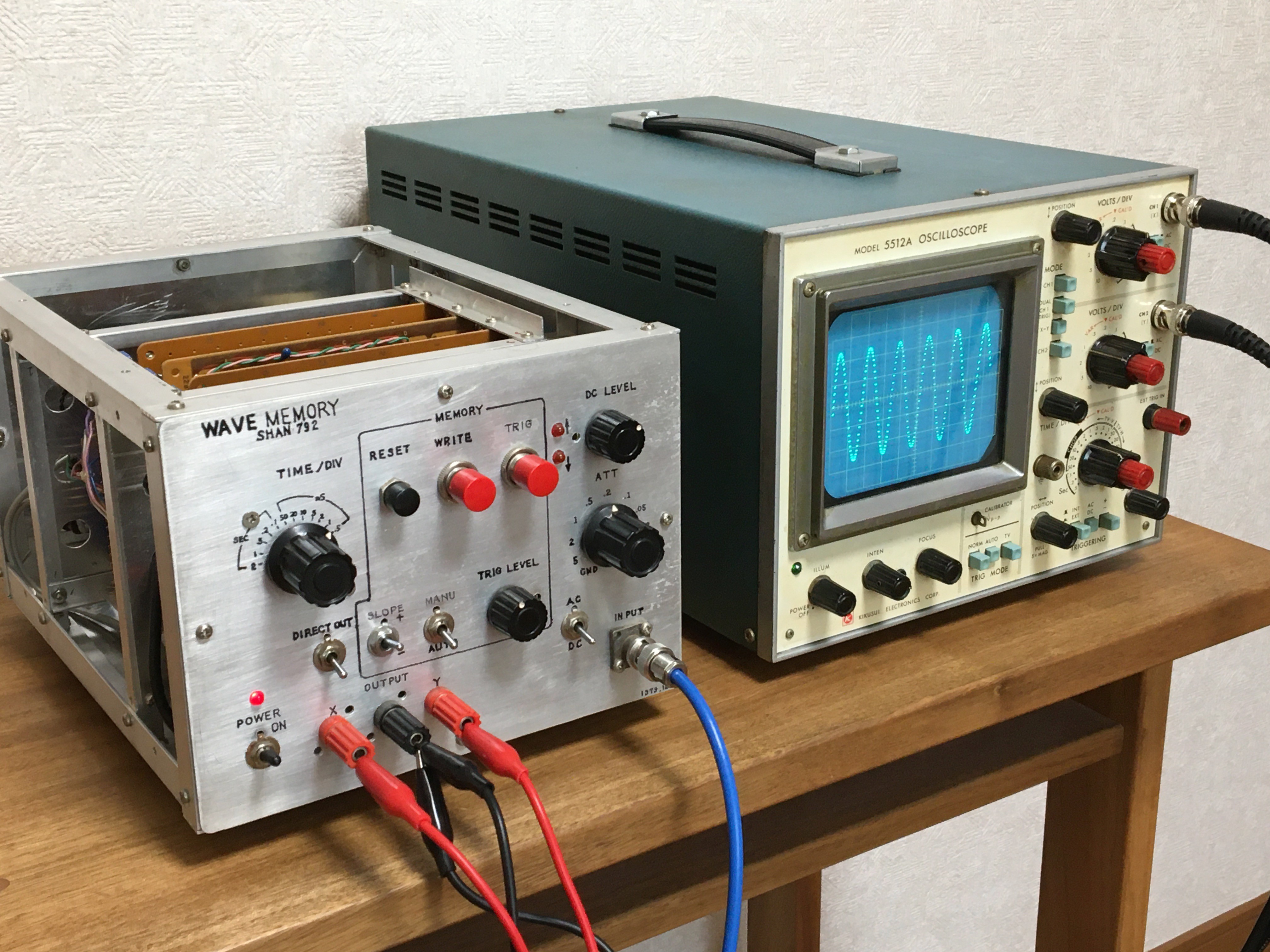
Fig. 1 Appearance of this Digital Sampler.
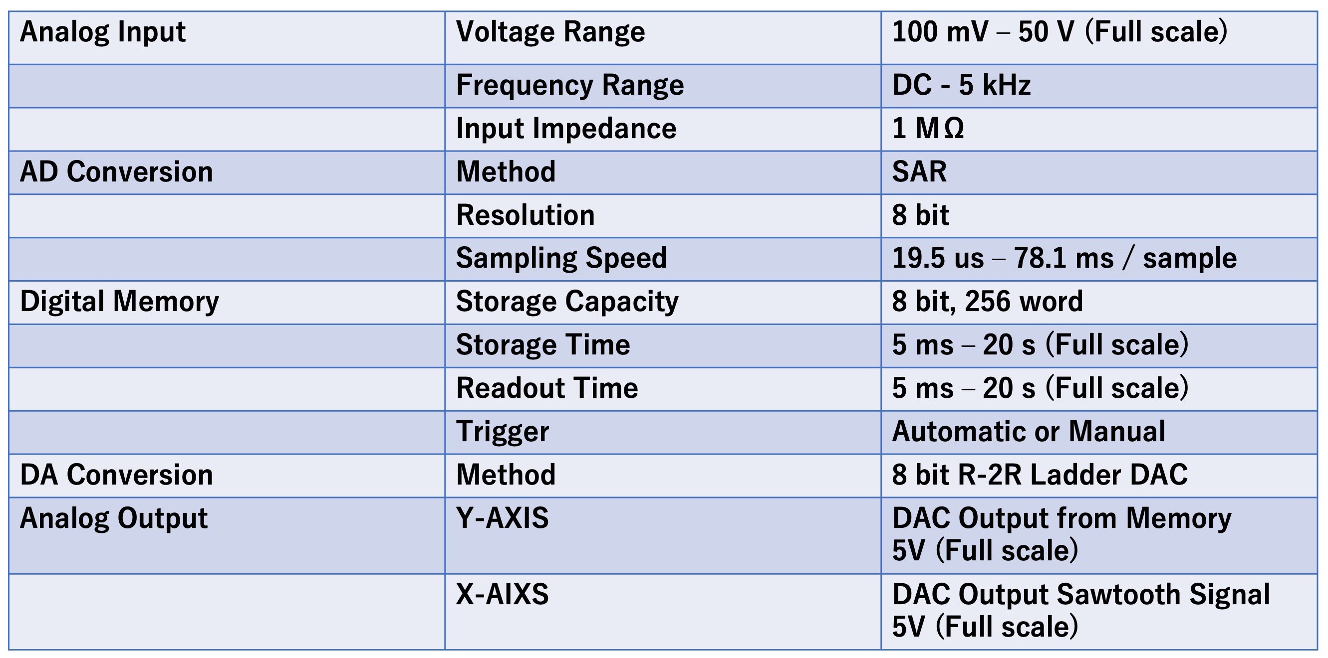
Table 1 Specifications of this Digital Sampler.
2. Operation example
Video 1 below shows a basic operation example of this Digital Sampler. The input analog signal is the signal from the function generator on the left side of the screen. The analog signal is sampled and stored by the Digital Sampler and displayed on the analog oscilloscope on the right side of the screen. The 500 Hz input signal is sampled with a sampling period of 39 us. And we can see that the input attenuator and DC level adjustment changes the over-range LED display. And it can be seen that the signal level at the acquisition start point on the left end of the oscilloscope waveform changes as the trigger level is adjusted. Then, when the Write button is pressed, the stored signal waveform is displayed in steady state.
Next, I will show how the display changes when the input signal frequency is increased from 500 Hz to 2 kHz and when the sampling rate of the Digital Sampler is slowed down. Furthermore, the frequency of the input signal move to set 24.5 kHz, which is almost the same as the sampling period. You can see that the alias phenomenon caused by the Nyquist theorem results in the display of a sine waveform that does not exist. The last part of the video shows sampling with square wave and ramp waveforms.
Video 1 Introduction of actual operation examples of the Digital Sampler.
(This video does not have audio commentary, so please turn on subtitles.)
3. Circuit configuration
Figure 2 shows a block diagram of the entire circuit.
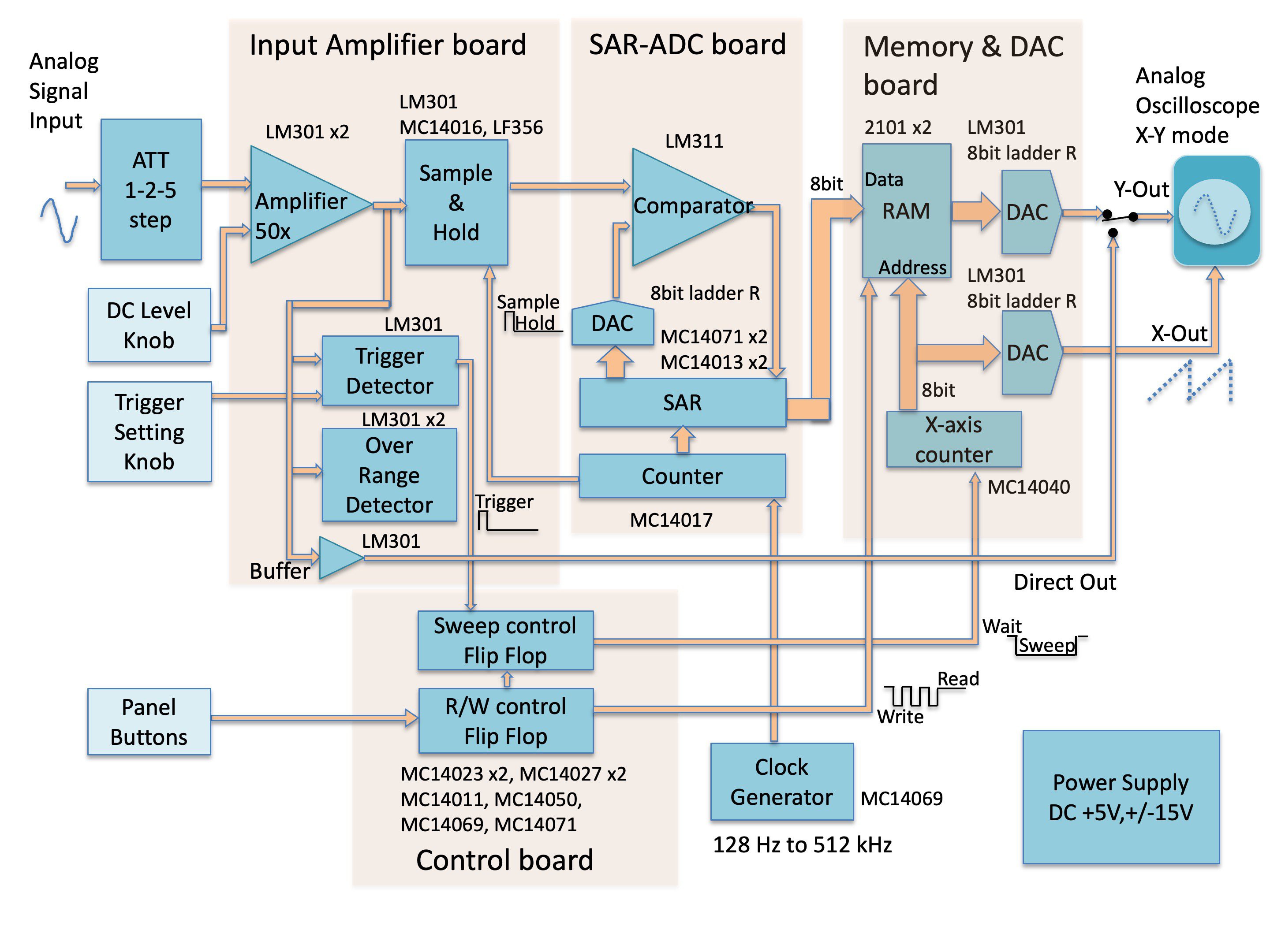
Fig. 2 Block diagram of the Digital Sampler.
First, the analog signal is adjusted to the appropriate amplitude with the 1-2-5 step attenuator on the panel knob. Then, the input amplifier board amplifies the signal with a gain of 50 times and performs sample & hold. The sample & hold is necessary because if the input voltage changes during AD conversion, the conversion result will not be correct. DC level adjustment of the signal, trigger detection and overrange detection are also performed on this board.
Next, AD conversion to 8-bit values is performed on the SAR-ADC board, using a SAR (Successive Approximation Register) ADC as the AD conversion method. Since inexpensive monolithic IC AD converters were not common at that time, the SAR-ADC was made by myself using discrete circuits. The sampling period could be switched in 12 steps of 1-2-5. The fastest sampling period was 19.5us, and the Nyquist frequency was 26kHz. Therefore, waveforms are clearly visible up to a few kHz. No anti-aliasing filter is provided.
After the 8-bit value of the AD conversion result is once stored in the memory IC, it is converted to an analog signal again by a DA converter and displayed on the oscilloscope. Here, the sampled signal is output on the Y-axis of the analog oscilloscope in XY mode, and the sawtooth waveform is output on the X-axis.
If the trigger mode is set to automatic and the trigger level is adjusted to an appropriate value, the input analog signal is stored in memory from the moment it reaches that value. 256 samples later, the bright spot returns...
Read more »

 danjovic
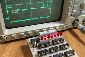

 Russell Kramer
 Clyne
Clyne
1979, the year I made my first synth with a 6800 !