Yann Guidon / YGDES
-
Be ready to change your opcode map a lot, until you can't
03/25/2019 at 15:07 • 0 commentsAs you might know, the opcode map is one essential element for the definition of a processor's ISA. At a single glance, it tells the programmer what the processor can do and how. It's like the cheat sheet for the rules of a game and it should be organised with binary/boolean logic (usually in 2 dimensions).
The opcode map is not only an exhaustive list of all the available opcodes. Think about Dmitri Mendeleev's periodic table of elements : the layout gives visual clues about the relative importance of various fields, for example. It tells the story of the processor's evolution (as is the case for the x86 family), hints at the design philosophy (or lack thereof), and you can immediately estimate qualities like orthogonality. And like with the periodic table of elements, you can spot holes (undocumented opcodes ?) or irregularities.
This is why the opcode map is also one of the precious tools of the designer. First, the map indicates the internal logic of the decoder and hints at implementation choices. Furthermore, the opcode map can highlight design flaws and its fill ratio indicates how much margin you have, or how many bits are underused, or how complete the design is...
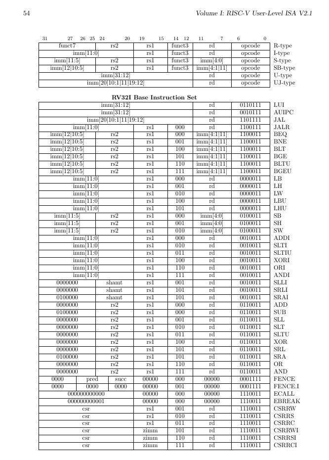
A little example of this principle can be found in the RISC-V ISA summary sheet. A quick look at the conditional branch instructions (BEQ, BNE, BLT, BGE, BLTU, BGEU) shows a gap of 2 opcodes between BNE (funct3=001) and BLT (funct3=100).![]()
Given the incredible degree of optimisation of this design, this gap is surprising so we can infer that 2 codes are reserved for extensions, for example.
Anyway the perfect ISA doesn't exist. It's always a compromise...Don't hesitate to move things around, rename, re-organise the fields during development. The fields and opcode names can change as the architecture is more clearly defined. Renaming an opcode is a matter of grep'ing through all the files and replacing the old with the new occurence. Changing or resizing a field can be more complex but the end user is shielded from the details by the assembler and the simulator. Write and design self-tests to ensure all the definitions are coherent.
Massage, optimise, allocate, polish as much as you can, as long as you can ! Because one day, it will be too late and the design will be used by others who can't afford the luxury to change the processor's fundamental definitions. It's much better to break things before they can have any impact on users.
Computer design history is already full of anecdotes of bad design choices that backfired. Take all your time to refine your design, element by element, test all the changes and allocate yourself a lot of margin so you can break/change definitions as needed. It's not possible to get a design right at the first try and you must iterate many times !
-
How to name opcodes ?
12/29/2018 at 20:03 • 0 commentsOh, what a wide ranging subject...
-
More condition codes
12/27/2018 at 09:36 • 0 commentsCondition codes are notoriously bad. Log 21. Conditional execution and instructions doesn't even scratch the whole subject but my latest "trick" is worth a whole log.
During private discussions with @Drass about the memory granularity, I realised that unaligned access was probably handled in the YASEP with the wrong perspective. When doing an insertion or extraction of a 16-bits word in a 32-bits architecture, the instruction would set the Carry flag to indicate when the extracted sub-word overlaps the natural memory word boundary. This way the program can detect if/when more code must be executed to fetch the remaining byte from the next word.
It's a little harmless kludge but it works in theory. Unfortunately this is not scalable. This wouldn't work with #F-CPU for example.
Enters 2018 and new insight.My CPUs typically have the following condition codes or flags :
- Carry (for add/sub/comparison)
- Zero (the result, or the register, is cleared)
- Sign (the MSBit of the register is the sign, useful for shifts and giggles)
- Parity (odd/even is the LSBit of the register, quite useful as well)
Today's unkludging is an extension of the parity bit : more bits are created that provide information about alignment before the fact, unlike the IE method. It also simplifies the logic for carry generation (I don't know why I chose to modify this bit in particular, and not the Parity bit)
In summary:
- For your 16-bits CPU, you just need the P flag.
- For 32 bits, you also need an extended parity that is a OR of the 2 LSBits, so you would have flags P1 and P2.
- For 64 bits : same again, you would have P1, P2 and P3, that you can check before any access to a Data register.
This is "good" because:
- Usually, to perform the same function, you have to issue a AND instruction with a bitmask (1, 3 or 7 for example) which adds some latency to the program and requires a temporary register to hold the result.
- The results of the ORing for the LSB can be stored in "shadow" bits that can be placed closer to the branch decision logic.
- You can test the pointer before using it, instead of after the fact
- The instruction decoder could eventually trap before emitting the unaligned instruction.
The less nice part is the increased coding space required in the instructions, to hold 1 or 2 more codes.
-
Coroutines
08/28/2018 at 04:23 • 3 commentsA discussion with an old-timer reminds me this coding technique for cooperative threads.
Coroutines are not used anymore because C and other languages don't allow this structure, so few people bother today... Yet they are still very interesting.
(more about them later)
...
-
I have a DWIM...
08/06/2018 at 20:10 • 0 commentsThere is no such thing as a DWIM.
DWIM = Do What I Mean
It's the classic "joke instruction" which illustrates why computers are so "unnatural" to mere humans : they can't do telepathy and they require clear, unambiguous and effective code sequences, using instructions that they already have, operating on data they can reasonably manage...
When creating an instruction set architecture, simplicity is the rule. Unless you design an application-specific processor (such as a DSP), stick to the very basics. Don't include an instruction that requires a logic diagram you can't easily draw on a napkin and find the lowest common denominator to prevent duplication.
If you're familiar with the RISC methodology, this sounds obvious, but most beginners (including me...) want to include "their instruction" because they don't know how to use the existing methods. Have a look at the Hackmem and similar "programming tricks" :-)
-
How to design a (better) ALU
04/12/2018 at 23:34 • 0 commentsAs @Martian created his new architecture #Homebrew 16-bit CPU and Computer, he credited this PDP project for ideas and guidance. In return I take the opportunity to comment on his ALU, which contains typical "misunderstandngs" that I have seen in many other "amateur" designs. These are harmless in a SW simulation but their hardware implementation would be significantly slower, larger and less efficient than what can be done. So this is not at all a criticism of Martian but a little lesson in logic design which, by the way, explains HOW and WHY my own CPU are organised in their precise ways.
Note : ALU design is already well covered there : http://6502.org/users/dieter/ This is a MUST READ but it might focus on particular technologies and here I'll cover some required basics.
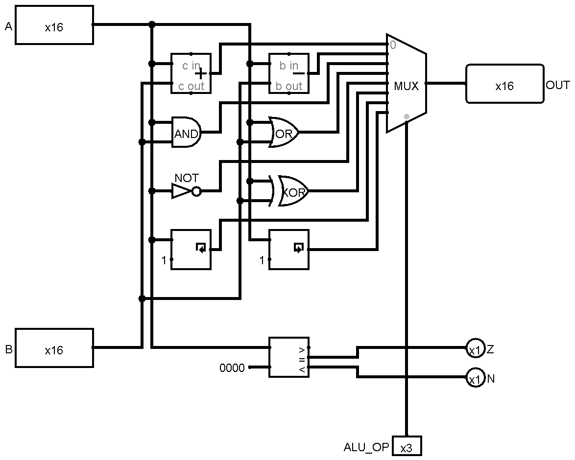
At least, Martian's ALU is very easy to understand : there is a big MUX that selects between many results of computations. One input for every opcode. It's large, the many inputs imply a very large fan-in and there is quite a lot of redundancy. See https://hackaday.io/project/131983/log/143820/ :
![]()
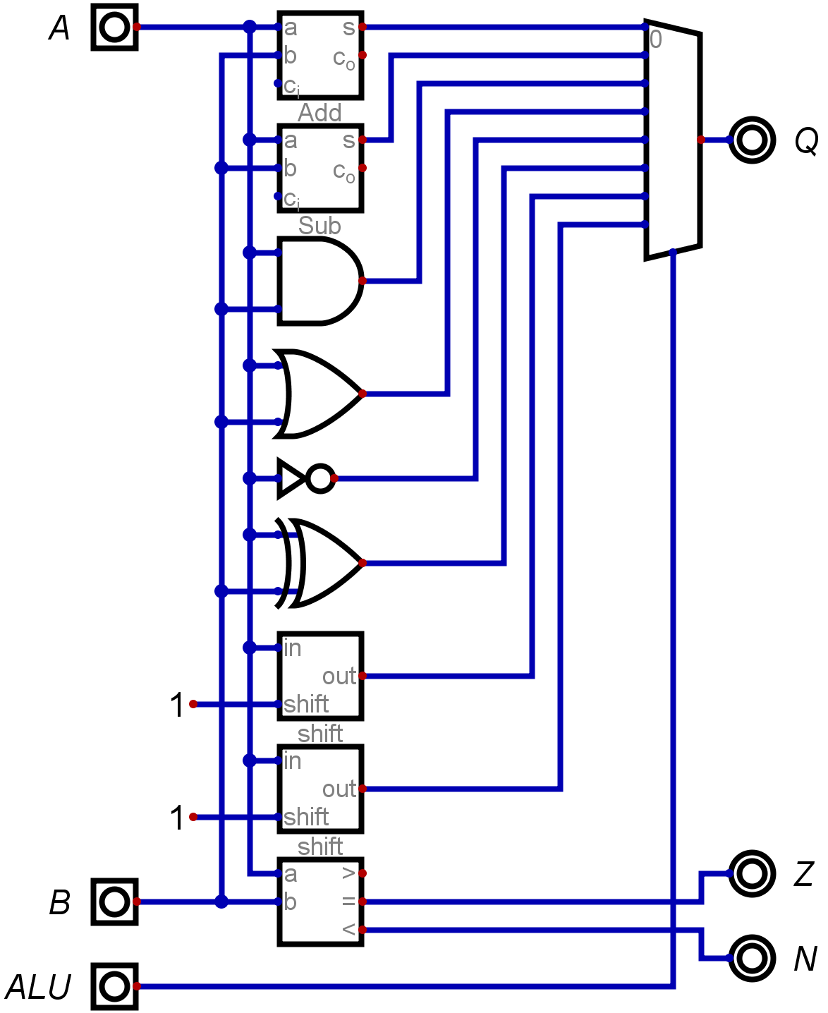
Another version:
![]()
So the name of this game is to factor operations.
I'll simply start with the elephant in the room : addition and subtraction.
In typical code (think C/Verilog/VHDL), you would write something like :
if opcode=ADD
    then result=ADD
    else result=SUB
if opcode=ADD then result=ADD else result=SUBWhich synthesises into one ADD block, one SUB block and a MUX2. This would be OK if the opcode signal came late but in this case, the opcode is the first thing that we know in the pipeline. The cost is pretty high, because ADD and SUB are actually very very similar circuits so only one is actually required.
The key is to remember that in 2s-complement :
C = A - B = A + (-B) = A + (~B) + 1
C = A - B = A + (-B) = A + (~B) + 1
so if you want to compute C, you need to
- invert all the bits of C (a row of XOR does the trick)
- increment the result
Oh wait, that's another addition unit added to our critical datapath... But sweat not. Since it's only 1, there is another trick : set the CARRY IN bit.
Tadah, you have it : a unit that contains only one carry chain and has the same critical datapath as a MUX-based ADD/SUB, but with
- almost half the parts count / surface / power requirement / etc.
- half the fan-in (because only one ADD is fed)
- a bit more speed
And this is just the first of many tricks in the book...
Another unit in the diagram is a "comparison" block. Which is... well, usually, a subtractor. The carry-out and/or the sign bit of the result will indicate the relative magnitude. But we already have a subtractor, right ? Just execute a SUB instruction and don't write the result back. That's it.
OK so now there is this row of XORs in the critical datapath. Is it a curse or a blessing ?
Actually it is welcome because it helps to factor other operations than the ADD/SUB. In particular, some boolean operations require one operand to be inverted : ANDN, XORN, ORN
So you only need to implement OR XOR and AND and you save even more units (and you reduce the fanout).
But wait, it doesn't stop there ! There is even more factoring to do if you are brave enough to implement your own adding circuit. And I discovered this trick in one of the historical FPGA CPUs more than 20 years ago.
A typical adder uses a "carry-propagate" circuit where two input bits of equal weight are combined to create a "generate carry" signal and a "propagate carry" signal. Both are the result of a very simple boolean operation :
- Generate is created by AND
- Propagate is created by OR
See what I see ?
These operations can be factored and shared between the adder unit and the boolean unit. The only gate to implement separately is XOR... which can be derived from the already computed OR and AND ! This XOR is in turn used in the last stage of the adder.
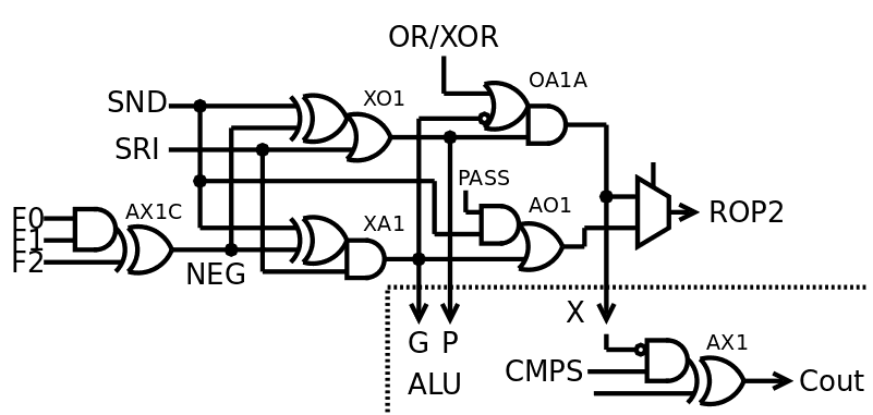
This method is implemented in the ALU of #YGREC8 at the gate level and it works very well. Look at the VHDL source code and the logs :-)
![]()
This diagram doesn't look at all like those at the top of the log, but now you can see why and how it is more efficient.
-
Divide (your code) and conquer
02/26/2018 at 23:00 • 0 commentsThis log is about a particular microkernel approach.
One important result of my explorations is to keep code small and well defined and turn the knob of the GNU HURD all the way up to 11 : "everything is a server". This has been studied with the #YASEP Yet Another Small Embedded Processor and resulted in the creation of the IPC/IPR/IPE trio of opcodes.
Ideally, any program would be split into chunks of about 64KB of instructions. The only way to communicate is to call the IPC instruction (InterProcess Call) with the ID of the called process, and an offset into the code. This call is validated by the IPE (InterProcess Entry) instruction, on the called code, which saves the callee's information in registers so the called code can accept or deny execution of the following code. IPR (InterProcess Return) is called to return to the callee's context.
This is a clear separation between code domains. This should prevent both the Spectre and ROP (Return Oriented Programming) types of attacks. This might look a bit slower than the "direct call" approach (as used in Linux "because it's faaaaast") but when well implemented, it shouldn't be much slower than a CALL within a process. It just exposes the costs of jumping from some code to another, without microcode or stuff like that.
So I advocate the following : split your code into small bits, for security and safety. Make them communicate with each other with protected calls to prevent mischief. This also promotes maintainability, modularity and code reuse, in an age of bloatware and executable programs that weigh many megabugs, I mean, megabytes...
Of course, this requires special instructions and a total rewrite of the operating system. Which means that current applications must be reviewed and there is no direct path to port GNU/Linux stuff. OTOH, the POSIX model offers little intrinsic security...
Another aspect to this is : separate processes with private data spaces need a SAFE, efficient, simple and flexible way to exchange blocks of data. This is a subject for a future log...
-
TTA - Transfer-Triggered Architectures
02/25/2018 at 12:10 • 0 commentsWe can find some TTA processors on Hackaday.io, such as #TD4 CPU so the idea has a low barrier of entry. It was also once considered for the early F-CPU project. Some commercial processors, such a Maxim's MAXQ, exist.
One advantage I see is : along with a VLIW approach, it could potentially handle OOO inherently, with low overhead. However, code density might not be good enough and people are not used to TTA idioms so on-the-fly binary translation from more classic RISC instructions sounds like a nice compromise. However this raises the complexity and increases latency, for an unknown gain in ILP, so a simple RISC (even superscalar) would work better in the beginning.
I also think that the system presented in https://web.archive.org/web/20071013182106/http://byte.com/art/9502/sec13/art1.htm is pretty under-efficient... I object that the very large crossbar bus that adds significant load (and surface), slowing down the whole (been there with FC0). There is also some redundancy, in even a simple case where you want to perform an addition : the 3 instructions contain the meaning of addition 3 times, in the 3 addresses of the source and destination registers. OTA mentions addition only once in the opcode...
TTA makes sense in a VLIW system, with some clever partitioning (to reduce bus complexity and fanout/fanin), which is already inherent in OTA architectures. This is why YASEP and YGREC are somehow a mix of OTA (for basic operations) and TTA (for memory and instruction control), they use the best approach for each case where it makes sense.
Oh, and how do you handle faults, context swaps, and register backup/restore in general ?
PDP - Processor Design Principles
Distilling my experience and wisdom about the architecture, organisation and design choices of my CPUs