Background: The original idea was (still is...) to build an electroerosion machine, so the specs for the power supply tried to accomodate that.
The first idea was to try to buy one, but Power supplies of this "power budget" are not easily available, are mostly "custom", and cost quite a lot of money. So I decided to build it, there are many Application notes available from many vendors, it seemed affordable. First mistake.
Dealing with High currents is not an easy task. For instance, if you have to test 30Amps/30V, you need a 1 Ohm load capable of handling 900W. It is not available "on the shelf", and costs some money. And also High Voltages are not easier to deal with, neither "pleasant" to feel. Errors in this environment are costly: I will publish the pictures of all the elements I burned: IGBTs (MANY), ATtiny Trinket, resistors, capacitors, ICs, etc. :-)
So, the problem became evident: what I was going thru, might be a problem for MANY hobbysts, if not ALL. Handling high power is complex, expensive and dangerous. No chance to use the simplicity of AnalogWrite() in this environment. So the idea was taking shape: not to build "another" power suplly, else build one that could work as a "power transformer" for an Arduino (for example) Analog output (PWM), so the designer only focuses on the application itself, he/she is isolated from the problems of high power, the high power could be handled via AnalogWrite() commands.
My guess is that the "in"famous Internet of Thiings will require to handle every type of "things", not just small ones, so handling high power might be something required quite often, if we are able to make it easily and affordable...
So, we have an Input of 5V, PWM, few mWatts, 490/1KHz, and we have to transform it to 60/90VDC (or any other), PWM (same duty cycle as the the input), 30KHz, 2KWatts.
I decided to go to an HBridge Architecture, if any of the "inhabitants" of this space reads this project, and is interested in understanding the reasons why I choose this design, I can explain it, not a problem. As a summary, I could say it is mainly the result of many constraints: the IGBTs SOA, the magnetics design considerations (I even had to build the ferrite transformer), the applications needs (isolation), etc.
The current status of the project is:
- final drawings (schematics and pcb): not finished yet, on the works, probably can finish them next week
- IGBT´s driving circuits: tested, design changed to optoisolated drivers (after burning many non isolated ones)
- output transformer: designed and built (2 prototypes, the ones in picture). If the calculuus was OK, the first ones are calculated for 48V Vout. The idea is to have several winding configurations available, the most usual ones.
- controller code: the multiphase clock is done and tested, it can also be adjusted with an external potentimeter. I am not an experienced programmer, so I need to learn some basics on how to share the code before being able to share anything...
- pending: reading the input PWM signal, and identifying frequency and Duty Cycle. Unfortunately, the Attiny85 has no ICP.
- Integrate the pieces
- everything is "first cut", will need extensive testing
- If Adafruit accepts it (need to check), the idea is to promote it as a "2KW Trinket shield" (the first one of its kind :-))
any idea is welcome...
Functional description:
there are 2 signal inputs: the PWM one (a digitual input), and an Analog input. This Analog Input (I called it Duty Cycle input) might be conected to a potentiometer, so you can actually reduce by an additional factor the Duty Cycle of the PWM signal.
This may allow to have a variable output Power supply, turned on by a continuous HIGH level in the PWM input pin (more than 2 or 3 times the expected clock cycle...). In the same way, if the PWM level (or the Analog level) goes down to zero, the power supply turns off. These might also be the "entry points" for the external mechanisms to be provided for current limiting.
Other possible Applications:...
Read more »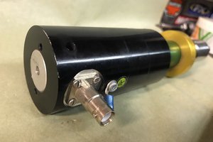
 JasMoH
 Denis
Denis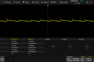
 hesam.moshiri
 Rue Mohr