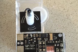
Close
0%
0%

GPS Disciplined xCXO

A DIY GPS disciplined 10 MHz reference clock

Similar projects worth following
In working on my Crazy Clock project ( https://hackaday.io/project/5880-crazy-clock ), one of the things I needed to do was make a very, very accurate frequency counter. That problem effectively reduces to the problem of making a very, very accurate square wave generator (the rest is relatively easy).To make a long story short, it occurred to me the other day that having a separate generator of a very, very accurate and long-term disciplined 10 MHz square wave would be a handy thing in and of itself, so I decided to design one as a separate standalone project.There are commercial GPSDOs available, and they're easily half an order of magnitude more stable than mine, but they're also much, much more expensive. My design is close to an ADEV of 1E-10 for the TCXO version, or 1E-11 for the OCXO version (which costs $100 more).

My first cuts at the crazy clock calibrator were using TCXOs with two different firmware loads. One load would test the clocks, the other load would accept a GPS PPS signal and would display the oscillator's drift relative to GPS. I could then subtract that drift out of the measurements of the clocks.

I tried to think of ways to allow the controller to do both at once. After all, a PPS signal (in principle) shouldn't distract the controller too terribly much. The problem is that the ATMega328P controller I like to use has only one input capture pin. Recall that the input capture pin allows you to use a non-prescaled timer (running at the system clock speed) to time things at maximum resolution, while the clock's value will be "frozen" by a rising edge on the ICP pin.

Since you can't watch two events at once with a single ATMega, it briefly occurred to me in a humorous way to simply use two. But in a "ha ha only serious" moment, it immediately occurred to me to simply separate the two problems - resulting in a frequency counter with a separate clock source, and a hyper-accurate disciplined clock generator.

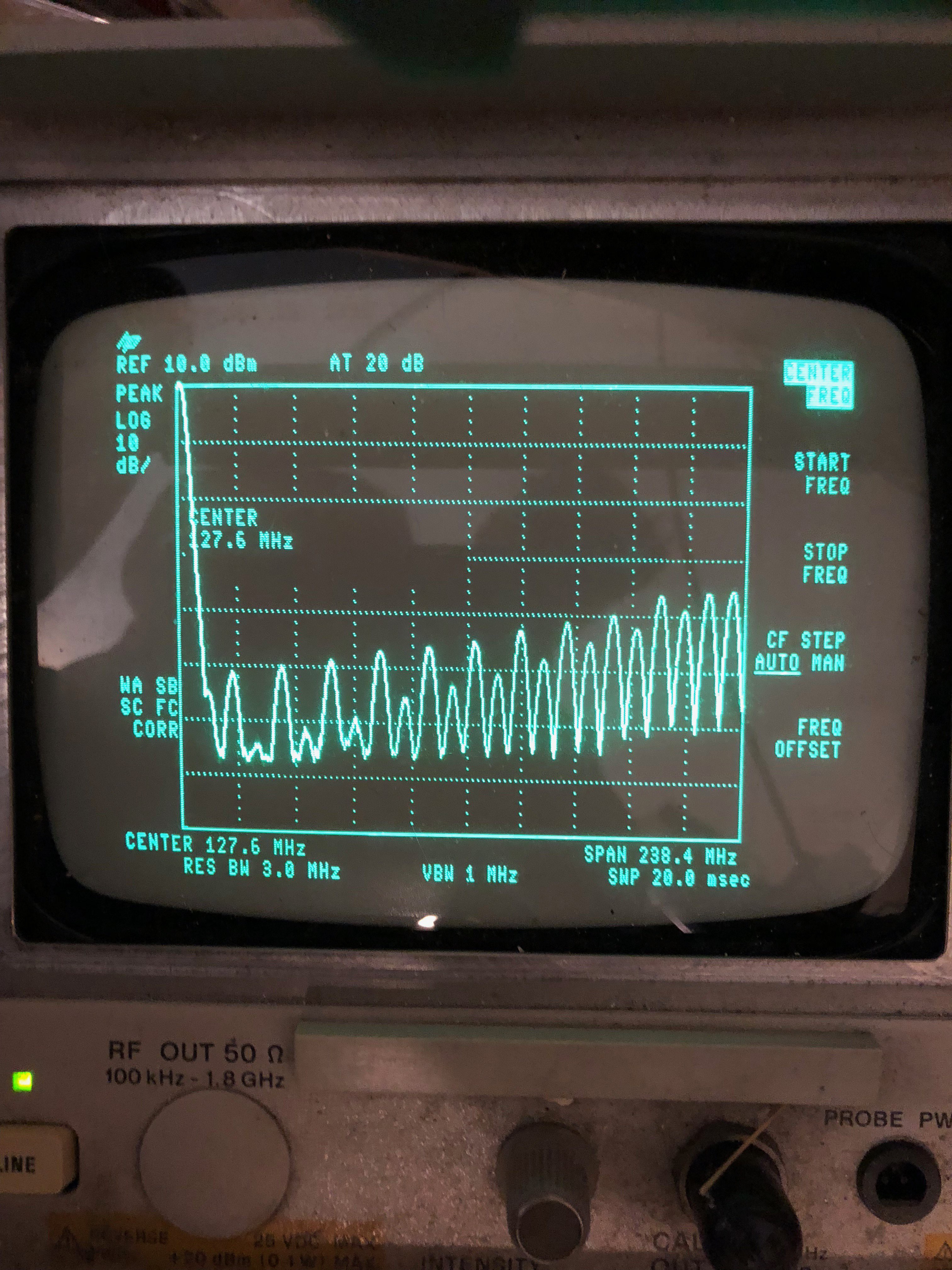
The basic design of the project centers around either a VCTCXO - a Voltage Controlled Temperature Compensated Crystal Oscillator or a VCOCXO - a Voltage Controlled Oven Controlled Crystal Oscillator. At first, that nomenclature seems contradictory. Which is controlling the oscillator? A voltage or the temperature compensation? In fact, what a VCTCXO is is a normal TCXO (a crystal oscillator which is "steered" by a temperature compensation circuit) with a voltage input that allows the output frequency to be trimmed over a relatively narrow range. The specification of the oscillator says that a voltage ranging from 0.3 to 3.0 volts will push or pull the TCXO ±10 ppm or the OCXO ±400 ppb. A VCOCXO is like a VCTCXO, except that the crystal is housed in an oven that tightly controls the temperature of the crystal. OCXOs are much more stable than TCXOs, but the oven requires a great deal of current.

The microcontroller is going to need to be able to manage the control voltage to trim the frequency from the GPS feedback. I briefly considered using the traditional Arduino method of PWM duty cycle manipulation to effect a D/A converter, but quickly rejected that. The TCXO has a basic short-term stability of 1 ppb. If we want to try and keep it in trim, we need to be able to have at least that level of granularity of control, preferably much less. We're already using the 16 bit timer for measuring the frequency. If you do the math, a one volt change in the reference is 7 ppm (or so), meaning that dividing our 2.7 volt tuning range into 256 levels results in a granularity of ~70 ppb per step. That's not nearly good enough. Using a 16 bit D/A converter, by contrast, gives us a granularity of just under 0.4 ppb. We can do better than that, however, because the outer 0.3v of the DAC range is "dead space" to the oscillator. Also, the long term accuracy specification of the oscillator lists < 5 ppm of total, lifetime drift. That means we can throw away half of the DAC tuning range (the outer 25% on the top and bottom) and still be able to steer the oscillator more than its lifetime expected error range. That doubles our granularity to around 0.2 ppb.

Connor Winfield has an application note that actually includes a schematic for a D/A trimmed oscillator. We started with that design, but a lot of the things they recommend have gone by the wayside. Their design included a buffer OP amp. Along the way, we turned that into a compression amp, but the design now is simply a voltage divider consisting of just 3 resistors. The aim of the voltage divider is to reduce the range of the DAC to the useful portion of the oscillator's control voltage input. For the TCXO, we reduce the swing to 50% of the 3.3v DAC output range, and for the OCXO, we reduce the swing by around 25%. But in both cases, we want the center of the range to remain...

Read more »

Adobe Portable Document Format - 121.84 kB - 02/18/2022 at 22:33

Preview
Download

sch - 524.48 kB - 02/18/2022 at 22:33

Download

brd - 206.12 kB - 02/18/2022 at 22:33

Download

Adobe Portable Document Format - 91.50 kB - 12/12/2021 at 18:58

Preview
Download

sch - 366.59 kB - 12/12/2021 at 18:58

Download

View all 21 files

  • FE5680 variant power supply

    Nick Sayer02/28/2022 at 01:24 0 comments

    The AP63205 has fallen victim to the supply chain crisis and won't be available until 2023, apparently. 

    It turns out that there is another option - the AP62200WU. It's not at all pin compatible and is an adjustable version, so you need a voltage divider to set the output voltage.

    I tried a board out, but it didn't work straightaway. It turns out that you can't just tie the EN pin to Vin because the absolute maximum voltage is 6 volts on that pin. You're supposed to use it to do UVLO with a voltage divider. Fortunately, you can just leave it floating and it will be internally pulled up, which is fine. I also managed to connect the wrong PPS pin on the new GPS module. So this board will return to inventory once I get another order from OSHPark.

  • New GPS receiver

    Nick Sayer12/12/2021 at 18:56 0 comments

    SkyTraq has EOLed the Venus838LPx-T timing receiver module. Their new replacement is the PX1100T, which has a number of advantages. For one, it's a castellated edge module rather than an LGA-69 package, which is easier to assemble. On the firmware side, the serial baud rate is 115200 rather than 9600. Because the same port is used for transmitting the debug output stream, it too has to follow along to 115200, but that has the side effect of making it consistent with the NMEA pin.

    Curiously, the PSTI,00 message quantization error is consistently zero. I have an inquiry in to SkyTraq about that, but according to the datasheet the potential quantization error is much lower anyway. There may still be concern about hanging bridges (white noise quantization error can be averaged away, but when the error is of a consistent magnitude, it can't be), but without a correction message, there's nothing that can be done.

    A prototype with the relevant firmware changes is operating no differently than previous models did. I'll run an ADEV acquisition on it after it's been running for a couple of days to insure it's as expected. I don't have any particular reason to think it won't be.

    EDIT: SkyTraq says they will have a firmware update later this week for the QE message.

  • USB C

    Nick Sayer07/17/2020 at 03:33 0 comments

    The more I get to know USB-C, the more I like it.

    It turns out that I believe both iterations of this project can be successfully powered from USB-C power sources.

    The OCXO variant is fairly straightforward. Since it doesn't demand more than 1A @ 5V, there's no need to hook anything up to any of the pins other than the standard CCx pull-down resistors.

    The FEI variant is a bit more complex. USB C can supply up to 100W, but negotiating the high voltage power that we would want requires some work. Fortunately, there are some very good solutions available. The best I've found is the Cypress Semi CYPD3177. That chip is a power sink negotiator, but what makes it particularly good for us is that it's desired voltage and current are set with voltage dividers, so there's nothing to program or set up. There's a "fault" LED that gets added that will light up red if the supply is incapable of negotiating the desired power (15 volts, 2.25A). Otherwise, the chip will pull down on a P MOSFET gate to send power to the circuit, once it's properly negotiated.

  • Another iteration on output conditioning

    Nick Sayer07/06/2020 at 16:44 0 comments

    I've decided to try one more pass at improving the sine wave output. This will involve ganging two of the NB3N551 outputs together to improve the output drive (ditching the square wave output in the process), and using a coaxial output - a U.FL jack on the board and an SMA pigtail to the front panel.

    I anticipate that the result of this will be a very, very clean output with reduced load change sensitivity.

    This change can't readily be done on the FE56x0 board because it also supports the FE405B, which has an output frequency of 15 MHz. On that board with the 405 oscillator, the LPF suppresses the sine output entirely because the corner frequency of the LPF is too low. In principle, you could alter the components of the LPF to raise its corner frequency, but I'm too lazy.

  • More on output conditioning

    Nick Sayer08/05/2018 at 17:46 0 comments

    I've been talking to a recent purchaser of the OH300 GPSDO and he's got some expertise in RF and has made some very helpful suggestions for making the output a little bit cleaner. I'm going to try his suggestions and the result should be cleaner output. Note that by 'cleaner' we're really referring to the waveforms themselves. The frequency stability is unchanged.

    • Add additional bulk capacitance near the clock fanout chip
    • Add some capacitance to the CMOS output
    • Add a common mode choke to the twisted pair output leads

    The bulk capacitance adds additional bypassing to the clock chip, which results in improved stability of the voltage on the 5v digital rail. The extra capacitance on the CMOS output increases the rise time slightly, but tames the overshoot that's present, making for a more stable output. The common mode choke reduces ground loop noise that can happen between the two outputs. That common mode noise was the reason for the rising amplitude of the higher order harmonics on the sine output. I haven't duplicated his results just yet, but the other fellow tried all of that and got all of the harmonics on the sine output to under 50 dB down from the fundamental, which is good enough to score.

    As soon as I can duplicate these results, look for those additions to become a standard part of the design.

    Note that the 56x0 discipline board doesn't actually come with output wiring, so users of those boards will need to do the common mode choke themselves if they wish. Of course, if you just connect one output up to the board, that makes ground loops between the two outputs a non-issue.

  • Load sensitivity

    Nick Sayer06/11/2018 at 15:54 0 comments

    From my experiments this morning with the new 5 pole sine filter I've discovered that there is some degree of load sensitivity on the output. I've seen this in the past when disconnecting loads - sometimes the mode will drop one notch while the PLL compensates. But somewhat more disturbing is that if you put a 50 Ω load on both outputs at the same time, you'll see a small glitch in the sine wave at the rising edge of the square wave (the two aren't perfectly in phase because the sine filter adds some delay).

    Fixing this means either lowering the power supply impedance to the output buffer chip or adding more bypass capacitance for it. I'll have to play with it some more, but for now my best advice is  to use one output or the other.

  • Sine output part 2

    Nick Sayer06/10/2018 at 22:00 0 comments

    I finally had an opportunity to build the GPSDO with the 5 pole output filter for the sine output instead of the 3 pole. It was also an excuse to dig out my old spectrum analyzer.

    Here's the old circuit:

    You can see that the first harmonic is only about 35 dB down from the fundamental and the third is not quite 50 dB down.

    Here's the new circuit:

    Now that second harmonic is knocked right down under 50 dB. I'm not sure what's up with the higher harmonics starting to drift up, but I did have to compromise a little on one of the capacitor values. I'm going to buy a reel of a better fit and maybe that will help a little bit. But even that I think is an improvement. I believe the higher order harmonics are less distressing than the low ones for a 10 MHz reference output.

    Of course, on my scope it looks like a sine wave, but the old circuit did too since my scope only has 50 MHz bandwidth.

  • On the sine output

    Nick Sayer05/14/2018 at 00:03 0 comments

    I've had some feedback from someone who bought a GPSDO that the sine output isn't as clean as I thought, and it turns out that the reason why it seemed cleaner to me was that I neglected to take into account that I have only a 50 MHz scope. Well, 50 MHz is only the 5th overtone of 10 MHz, so my view on the output is a bit myopic.

    So I'm going to order a set of boards to try with footprints for a 5 pole filter instead of a 3 pole filter. That ought to improve the filter's performance a bit (hopefully enough).

  • Grand firmware unification

    Nick Sayer03/22/2018 at 17:03 0 comments

    I've built and tested a prototype of the XMega32E5 controlled OH300, and it works fine. This has allowed me to return to a single firmware source for both boards. In the source code, you include an oscillator include file that has a bunch of macro definitions to tailor the source for that oscillator. In particular, the two board types are differentiated by the SPI_DAC macro. The FEI boards do not define that macro, and the OCXO and TCXO variants (not sure if I will go to the trouble of designing one of those - they don't really sell) do. In addition, if SPI_DAC is defined, you can choose between the AD5680 and AD5061 DACs depending on whether you need 16 or 18 bits of resolution (16 bits is for the TCXO variant). Next, the oscillator control file is where you define the EFC GAIN and (for the FEI board) any BIT_REDUCE value required to bring the gain down to a useful range. Lastly, the file defines the two or three time constants to be used by the modes. Longer time constants trade phase control for frequency stability.

    If your oscillator has an inverse EFC slope (higher EFC means lower frequency), then you can change the DAC_SIGN value from 1 to -1. Other than that, there should be nothing in the actual source code to change.

    The source repository includes support for the FE-56x0A, FE-405B (using the FEI board), and the OH300, ECOC-2522 (using the OCXO board) and the DOT050V (using a TCXO board, but I may not bother designing one).

  • XMega FE-5680A board build report

    Nick Sayer03/19/2018 at 14:29 0 comments

    The XMega board variant arrived and the prototype built. Converting the firmware over to the XMega architecture was a tedious exercise, but the result seems to work pretty well. At boot the board sets itself up to clock from the 32 MHz RC oscillator brought down to 30 MHz. The DFLL uses the internal 32 kHz RC oscillator to tune it. Once the FE lock pin is asserted, the PLL is set up to triple the 10 MHz input and switch over to using that. This neatly avoids the whole problem of the clock instability causing controller lock-ups and malfunctions prior to physics lock.

    A side effect of this is that programming now no longer strictly requires the external oscillator be fed. PDI programming can take place regardless. Of course, that means having to use a PDI programmer, which is marginally less convenient for me than SPI programming.

    If there's a real downside it's that I've discovered the chink in the XMega's armor: the ADC is terrible. I've had to configure it for differential mode with the negative pin connected to ground internally. The result is effectively an 11 bit ADC instead of 12 bits, and even then it's so noisy that throwing away another bit to make the output compatible with the ATMega ADC doesn't matter - it still jumps around 2-3 bits worth even then. For our purposes, it isn't too harmful, though, as the phase discriminator output gets averaged over the course of many seconds. It's bad enough, though, that I may wind up adding another conversion to the capture ISR to get a two-sample average each second.

    I designed an OH300/ECS2522 board variant with the XMega too. It's not strictly necessary to convert that design, but the benefit would be the possibility of unifying the firmware across both platforms. The only real difference between them would be changing the serial oscillator interface into an SPI interface to drive the external DAC (the XMega has a 12 bit DAC, but that's not nearly enough granularity). Other than that, all that changes are some constant values relating to the EFC slope.

View all 121 project logs

  • 1
    Step 1

    Paste, place and reflow all of the components on the board.

    It may seem a bit harsh for that to be one instruction step, but there's really nothing particularly special about the process for this board. As always, make sure the polarized components are placed the correct way 'round.

  • 2
    Step 2

    Install 2 JST XH headers in the output port positions.

    If desired, install a mini-DIN 6 connector in the diagnostic port. One pin is ground, one is a copy of the PPS signal from the GPS module, one is the transmit data pin of the GPS module, one the the receive data pin of the GPS module, one the diagnostic serial transmit pin of the controller, and the last 2 are 5 volts and ground. You can send commands to the GPS module if you like, but altering the NMEA message structure or timing may cause the firmware to malfunction. The firmware makes no effort to update the UTC reference year, so the date stamps in the diagnosis log may wrap at some point in the future. This should not have any impact 

    For the FE-5680A board, add a DB9 female connector with PC board pins. It mounts on the edge of the board with the 5 top pins soldered on top and the 4 bottom pins soldered on the bottom. Bend the pins together slightly to make the mechanical fit better. Solder one pin and then examine the jack from the side to make sure it's straight before soldering the rest of the pins.

  • 3
    Step 3

    Using a pogo pin adapter and a PDI programmer, program the controller. Be sure your programmer operates at 3.3v. The XMega32E5 controller is not 5v tolerant.

    There are no fuses to set on the XMega controller. Just upload the code to flash.

View all 6 instructions

Enjoy this project?

Share

Discussions

wmeyer48 wrote 12/13/2021 at 18:12 point

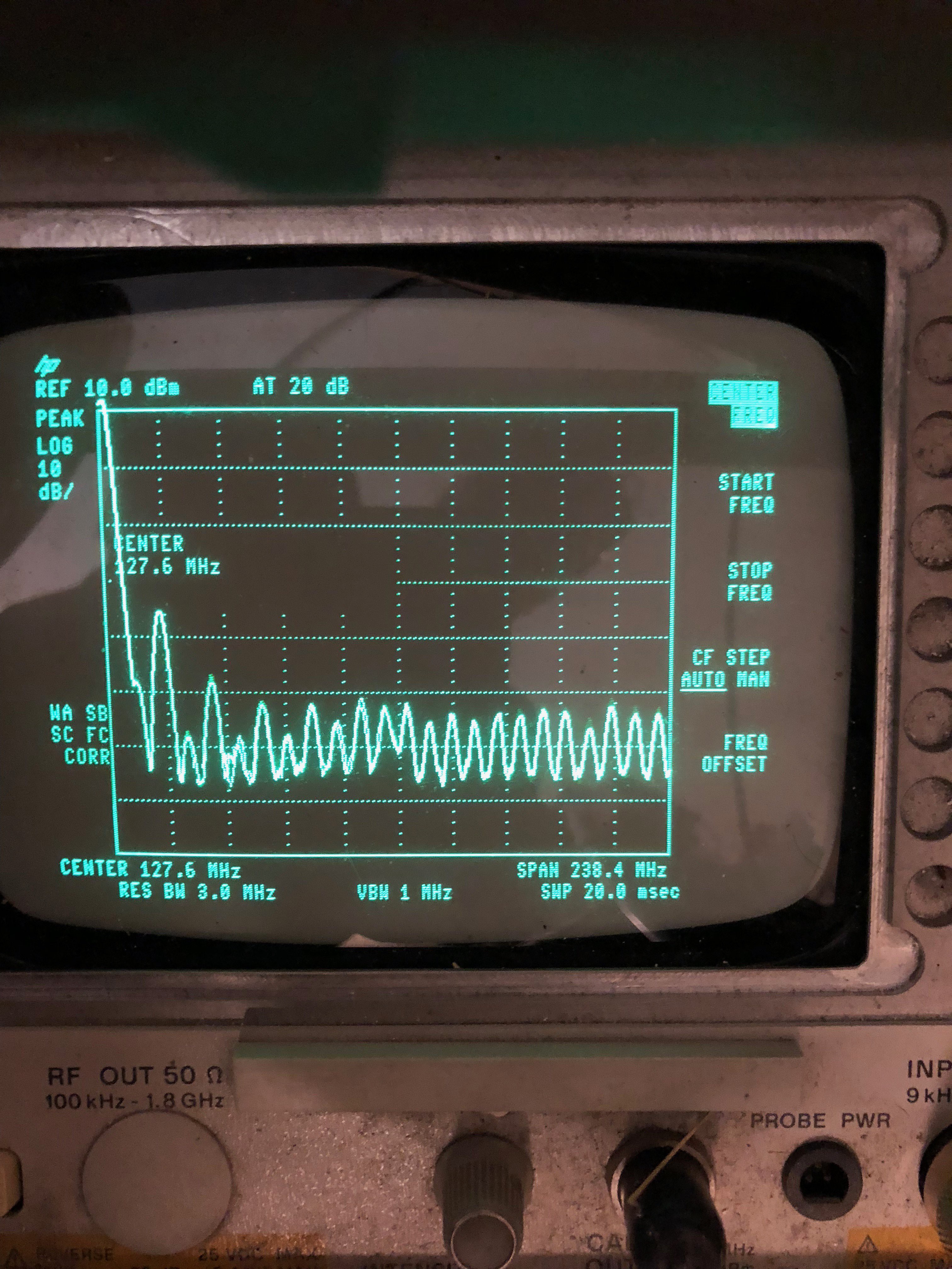
Interesting project. Many years ago, I tinkered with an oven controlled oscillator from a commercial television sync generator. They built their own oven, using a machined block of aluminum with a cavity to fit the crystal, another for a thermistor, a milled flat for a power transistor as heat source, and an op-amp to control the current source transistor.

One thing I noticed was that the oven, when not enclosed in its insulated metal case, was extremely sensitive. Monitoring the current to the heater, and blowing gently at the oscillator from about three feet away, the response was impressive.

If I were to tackle such a project, I would probably build the oven in a similar way, rather than buy a commercial package. More work, but the inevitable trade-offs would be mine to make.

  Are you sure? yes | no

Nick Sayer wrote 12/13/2021 at 18:15 point

You're correct about OCXOs still being sensitive to temperature changes. My lab is an unconditioned garage and I do see diurnal EFC drift. This may result in aggravating the medium term ADEV, but thus it has ever been, so my results probably represent a worst case.

Of course, I only test them in their cases. Things are worse if you test them as a bare board. The air space inside the case surrounding the OCXO provides some level of insulation. 

  Are you sure? yes | no

wmeyer48 wrote 12/13/2021 at 19:08 point

In the sync generator I used as a reference, the oscillator had the inertia from the chunk of aluminum, and was protected by layers of styrofoam inside the steel case, but in addition there was a case cover on the backside of the PCB, with a layer of styrofoam between it and the PCB. And it still showed some minor sensitivity. But in its card cage, and the cage in a rack of equipment which was always operating, it was impervious to ambient changes.

  Are you sure? yes | no

project.director wrote 05/05/2017 at 04:52 point

Hello Nick..?

Ok Sir, I do not really know how to use this site, and I dont really plan on becoming a regular member. However, I have been working on a project for some time that is a timing and scoring application for off-road Rally Racing events....website is www.ohprg.com

I think that you have a couple of items, GPS Clock and GPS Time Server that will save me and my team hords of development time and effort on...not to mention money as we are all volunteers and dont get paid for any of this........

Im down in South Orange County, CA and VERY much look forward to speaking with you.....
I signed up on this site specifically to make contact with you.....

  Are you sure? yes | no

Joost Breed wrote 11/27/2016 at 20:53 point

Nick,

I noticed that you are using a switching regulator in your FE5680 design. Doesn't that add more phase noise to your signal compared to linear regulators? I'm currently using low noise LT1764A for all of my voltages, but they are a bit expensive, I need three of them. I'm wondering if you it is possible to make a low noise switching regulator.

Joost

  Are you sure? yes | no

Nick Sayer wrote 11/27/2016 at 21:11 point

The FE5680A datasheet has a spec for maximum noise and ripple on the power inputs. I sort of assume that if the power supply is better than that (and it is) that there's no benefit to be had in the output by improving the supply.

Using a linear design for the FE5680A is going to be a challenge because of the high current requirement.

  Are you sure? yes | no

Joost Breed wrote 07/29/2016 at 06:28 point

I could not reply to your last post. So I'm writing it here.

You have the wrong datasheet. That's the one of the P and L version. The T version has a 10MHz output on pin 12. 
http://navspark.mybigcommerce.com/content/Venus838LPx-T_DS_v2.pdf

I'll have a look at averaging out the jitter you wrote about and do some experiments. But what do you mean with 'the averaging window for the phase to the PI time constant divided by 4'? How does that work?

Joost

  Are you sure? yes | no

Nick Sayer wrote 07/29/2016 at 15:05 point

I wrote back to them and there's been some confusion.

There is a v4 datasheet for the timing module and the nav module. You are looking at v2 of the timing module, and I was looking at v4 of the nav module.

The actual correct datasheet is http://navspark.mybigcommerce.com/content/Venus838LPx-T_DS_v4.pdf

  Are you sure? yes | no

Joost Breed wrote 07/29/2016 at 19:54 point

That version also has a 10MHz output on pin 12.

  Are you sure? yes | no

Nick Sayer wrote 07/29/2016 at 22:41 point

That's true. As before, however, I'm not at all confident that it's stability is comparable to what you can get from an OCXO.

  Are you sure? yes | no

Joost Breed wrote 07/28/2016 at 18:34 point

Hi Nick,

I came across this project after googling my own project. I'm  just finished the first version of my reference (https://www.elektormagazine.com/labs/gps-assisted-10-mhz-frequency-reference). I actually like your idea of using a PLL with a current source. Do you mind if I use that part in my project?

  Are you sure? yes | no

Nick Sayer wrote 07/28/2016 at 18:51 point

That's absolutely fine. It's only fair, since I got the idea from someone else (Jim Harman), and he got it from someone else... So it's definitely tribal knowledge at this point.

You'll find that adding the phase discriminator will make initial lock-up *MUCH* faster and you'll see far tighter phase control. What you'll want to do is balance phase coercion against the resulting frequency (in)stability. In other words, the harder you try to keep the phase lined up, the more you have to horse around the frequency to do it. Finding a good balance (which really means finding the best PI loop time constant) is the task at hand.

I've taken a look at a your article, and have a couple of ideas for you. One is that to convert sine to square you might try using a self-biased inverter instead of a high-speed comparator. You can check out the FE-5680A variant of the GPSDO to see an example. It's perfectly suitable for the job and likely is a lot cheaper.

Also, I've been using the PA6H all this time, like you, but it's a navigation module rather than a timing module. Navigation modules can serve the purpose, but for adequate timing results you have to give them *really good* reception. Timing modules can survey their location and then run with only one or two satellites with the assumption that their position is fixed. Additionally timing modules can give quantization error correction data for their PPS pulses. That allows you to factor away the PPS jitter, obtaining PPS timing that's as good as is possible with GPS at all (maybe down to ±1 ns or so). I'm taking a look at the Venus838LPx-T timing module. It's an LGA69 device, so soldering it isn't trivial. I hope to make a breakout board for it available on Tindie soon.

Another thing you can do is trade out your 32 bit hardware counter for one of the timers in the Atmel controller. To do that, you need to trade out your controller break-out board for a bare controller and fuse it for an external oscillator and clock it directly from the OCXO. If you do that, you can use the input capture facility to directly count the number of cycles of the OCXO that happen between PPS pulses. Even with the phase discriminator, you need to be able to track that, because if the frequency isn't close enough to the correct number of cycles per second, then the phase will wrap (that is, the ADC value will go from high to low or from low to high as the phase angle crosses 0) and be very difficult to track.

Of course, all of that basically converts your design into my design, so maybe I should just shut up. :D

  Are you sure? yes | no

Joost Breed wrote 07/28/2016 at 22:09 point

Nick,

Thanks you for the tips. I can use those. Some of them I already implemented. I actually threw out the comparator last week and added a non buffered inverter with feedback resistor instead.

I also like the PA6H. Until now I was not able to find a GPS with less jitter. I measured the jitter and it is about 10ns. Do you use the average of multiple pll measurements to cope with that? The jitter must influence the pll output as well I guess.

I did not know about the Venus timing module. The module actually contains a 10MHz phase locked reference as well. I like it, but its a bit expensive, $50 or so. I like to keep it cheap. That's one of my goals. It will also be a problem for most people to solder the package. Although I own a home build smd oven. 

I was also thinking about using the internal counter instead of the external one. I used the external counter in this version because I was not able to check if the internal counter actually was counting correctly because of some latency. With the external counter I was sure it worked and also could measure that. Didn't you have any problems with any latency between the interrupt from the 1pps and storing the counter value? Or isnt't there any because it is not handled by the cpu?

Why did you swap the Atmega328p for the Attiny4313?

If I would use all your tips both our projects will look more or less the same I agree. But I don't mind, and I hope you don't. I'm having a lot of fun building it and figuring things out.

Best regards,
Joost

  Are you sure? yes | no

Nick Sayer wrote 07/28/2016 at 22:41 point

The way you can use the internal timer without latency is with the "input capture" feature. One of the pins on the controller (assuming you're using one that has the feature) will copy the current timer value into a holding register "instantly" and trigger an input capture interrupt. That facility allows me to accurately count the exact number of cycles of the system clock between rising edges of PPS. Since the timer value is captured in the capture register, the latency in reading it is immaterial (as long as you don't allow the value to be overwritten by the next capture).

I went with the ATTiny4313 originally to lower the cost. I may be going back to the 328 (actually the ATMega328PB) to get more flash space. I'm using the ATTiny841 now (to gain a 2nd USART and ADC), but I'm running out of flash.

My code sets the averaging window for the phase to the PI time constant divided by 4. This averages out the PPS jitter, but some GPS modules have a phenomenon called a "hanging bridge." See http://www.leapsecond.com/pages/m12/sawtooth.htm for an example. A hanging bridge can cause the averaging to be incorrect. Virtually all modules have PPS jitter because the microcontroller clock doesn't stay in phase with UTC, but it's only when the phase rate-of-change changes sign and the phase angle remains constant second-to-second for some period of time that there's trouble. Some GPS module select fractional controller clock frequencies to make *sure* that the phase rate of change never approaches zero for this reason. They don't have a problem because if you average the phase errors, they'll center around the actual value.

Timing modules will often provide you with a quantization error correction message. You take the observed PPS phase error and adjust it by the value of the quantization error. That gives you the actual phase error to the true UTC second. Hanging bridges and averaging are completely mooted by that.

I am not sure the Venus module's reference output is good enough to directly use for anything. I don't expect that its short term stability will come close to what an OCXO can deliver. It's certainly possible that it's better than I expect. I don't know. Also, I'm not sure that feature exists in recent versions. If you look at the latest version of the datasheet - http://www.skytraq.com.tw/datasheet/Venus838LPx_DS_v4.pdf - none of the pins are any sort of secondary frequency output.

  Are you sure? yes | no

Blecky wrote 04/07/2016 at 05:27 point

Hi Nick,

Are you looking to get these in stock again on your tindie store in the future?

  Are you sure? yes | no

Nick Sayer wrote 04/07/2016 at 05:41 point

Yes. Boards are being fabbed as we speak by OSHPark. They're due around tax day.

  Are you sure? yes | no

Blecky wrote 04/07/2016 at 06:15 point

Groovy, I've added myself to the wait list.

  Are you sure? yes | no

Blecky wrote 08/03/2015 at 05:23 point

±50ppb. Love that little VCTCXO.

  Are you sure? yes | no

Nick Sayer wrote 08/03/2015 at 05:26 point

It's actually much better than that. The ±50 ppb is its long term stability. The short term stability is ONE ppb. The long term stability is uninteresting in this case because of the feedback loop with GPS.

  Are you sure? yes | no

Blecky wrote 08/03/2015 at 05:50 point

Nice, you wouldn't happen to have the Allan deviation plot for this (I can't seem to find it)?

  Are you sure? yes | no

Nick Sayer wrote 08/03/2015 at 05:53 point

I don't have anything from Connor Winfield. I hope to be able to come up with something with the prototype of my design when the first boards arrive.

  Are you sure? yes | no

Similar Projects

Does this project spark your interest?

Become a member to follow this project and never miss any updates