BLEezy: Raspberry Pi Zero
An easy to use BLE module for the Raspberry Pi based on the nRF51x chipset
An easy to use BLE module for the Raspberry Pi based on the nRF51x chipset
To make the experience fit your profile, pick a username and tell us what interests you.
We found and based on your interests.

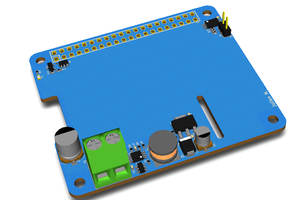
This isn't really an update on the project just a new image. I have wanted to be able to render KiCad files in Blender for a while but have never gotten around to it. I spent some time today to figure it out and this is the output. This is done using the cycles render engine. Hopefully I can make a more techy environment than just the gray metal.
I mentioned early on in this project that due to my locational status I was not really able to build things. To this effect I was hoping someone else would want to work with me on building and prototyping. Well someone found me who was very interested in building and guess what?? We already have some board! So lets take a look.
Check out the log on my blog OpenFet BLEezy
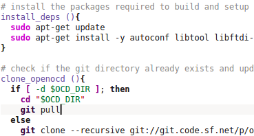
This board is all about the hardware but I want to sort out the software as well so its very easy to use. The first step was to get OpenOCD on the PI in a way that doesnt confuse people who are new to the Pi. So I created a simple OpenOCD installer script. The script will install all dependencies, clone openocd, build & install, and test the installation. The script is on github (oh yeah i moved the git)!
I dont have a Pi at the moment so if someone could please test this for me that would be great! it wont damage anything you currently have setup on your Pi.
Also this works on most Linux Distros and machines so it might be handy for your computer as well.
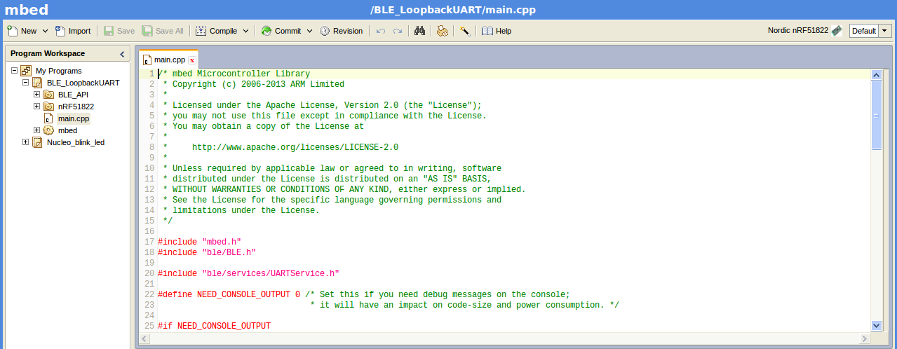
When I make something I generally go into it to learn something. Another thing I want to learn out of this project is how to make the toolchain simple. After some advice and poking around I have found a solution for programming the BLEezy. It will use mbed, OpenOCD and the Raspberry Pi. I have already written the installer scripts now I am working on the programming scripts.
(write project on mbed.com) -> (Download hex) -> (run python script to install hex on BLEezy) -> Done!
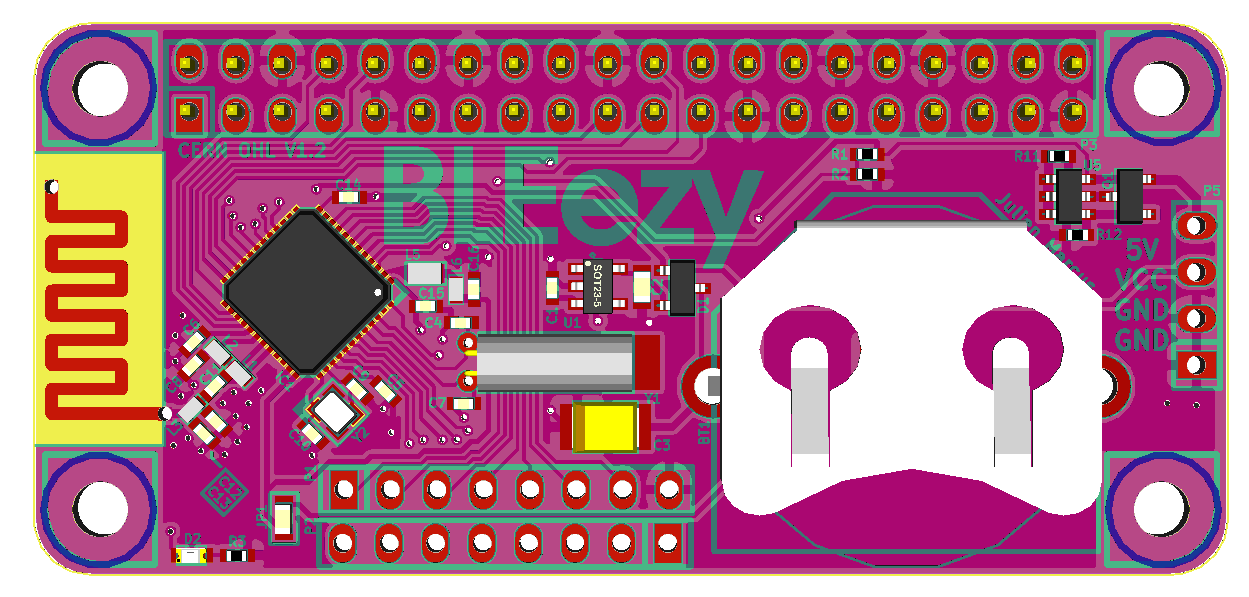
A valid point was raised that it would be better to have the battery on top for production. When I created this design I wasn't really thinking about production at all but it is good practice. And in the off chance that this product does go into production we wont need to make that change later and re verify the design.
Slowcoder has also joined the team. He will be taking a look at the routing and see what improvements can be done.
The git repo is now up with the up-to-date board design. The nRF components are verified. So if you would like to use the nRF chip in your project you can clone this repo and pull the part out.
The routing for the BLEezy module is now finished. All the components are placed and the additional header was removed. I am now working on double checking the programming interface and software with the design.
Create an account to leave a comment. Already have an account? Log In.
I've designed several nRF51x22 boards, and I just reviewed your design.
First off, it should work, so consider this "nitpicking", or whatever. :)
1. Routing on the back. There are several traces running on the back of the board, just where pins 30&31 of the nRF are on the top side. These pins are the outputs of the PAs in the nRF51, so they'll likely introduce a bit of interference in the traces on the back
2. No guard-ring around the 16Mhz crystal. It works without it most of the time, but it's just good design to include one.
3. Efficiency when powered using the coin-cell. You are using the internal LDO of the nRF51 to get the (internal) voltages down to 1.8V (and a few others, but those you cannot affect). This means that the difference in voltage of the battery (3.0V nominal) and the internal 1.8V is going to be bled off as heat. That means that 40% of the total capacity of the coin-cell will be wasted as heat. It should still last a good while, but it would last almost 40% longer by using a DC/DC buck-converter. (Hint: There's one built-in in the nRF51)
Edit/Addition:
I looked closer at the routing, and found that you could get a _much_ cleaner routing if you re-arranged your nRF-GPIO to RPI header mapping. Is there a particular reason to why you mapped it the way you did?
As far as I know, all digital functions (except SWD) can be mapped to any pin on the nRF51. The analogs are tied to P0.00->P0.06, of course.
If you'd like, I could take a stab at it
If I might get on the nitpick train for a minute...
*IF* you were to manufacture this, you'd be spending extra to have the battery holder mounted to the back. Simply pushing the power stuff closer to the IO header and putting the holder on the front would let you do all the SMT in a single load which would be cheaper on the assembly line.
I had it on the top at first but it made it made everything pretty tight. But that was before I removed that small 4 pin header. Ill take a second look at putting it on top. I could also use a smaller battery but the capacity would be much much lower.
I made a quick example of how I would have routed the analog and digital header (P1+P2).
Design filosophy: Keep as much as possible on the top layer, so that you can have a nice clean ground-plane on the back. If there's to be vias and traces on the back, keep them far away from the sensitive stuff.
I'm not familiar enough with the RPI header pinout to rearrange that right now. I could read up on it...
The RPi pinout holds over some legacy from the 26 pin first gen models and continues the philosophy of inconveniencing everyone and favoring no one.
Yeah that would be great! I learn a lot from your comments and I'm sure I
will learn a bunch if you do some routing as well. Ill make changes to
the .sch now and let you know when I'm done.
Hmmm my internet went a bit screwy with those last comments. Also I thought a guard ring is only necessary with a single sided board? Doesnt having a ground plane underneath connected closley to the cap ground to the same thing?
Nah, the guard ring is there to reduce capacitive coupling from near-by high-frequency traces. Nearby in this case is all 3 dimensions (RF isn't 2D).
Capacitive coupling can be an issue, as crystals are very low-power devices, so even a very small coupling can affect the stability of the crystal.
Now, things won't "stop working", but the frequency could drift a bit, causing issues with long-term stability.
Again, it's probably fine though, but for mass-production, I would have addressed it.
Now that I think about it, why not slap on a prefab module like the Raytac MDBT40: http://www.raytac.com/product_detail.php?id=38 ? If you want the adventure of doing the RF stuff yourself, then keep at it.
Otherwise it is way easier to solder down one of these and forget about the hard work and expense of implementing the antenna and FCC/CE certifications testing. Of course, if you wanted to sell these for any reason you'd have to also get a Bluetooth SIG certification which isn't done on a module basis regardless.
This module is $7.50 from Seeed and probably cheaper through Taobao / Aliexpress / markets. The nRF51822 quotes at $4.67 for the 48QFN -QFAA model, so by the time you add in the balun, main osc, and other discretes it'll be about the same price in components alone. The MDBT40 lacks the 32kHz crystal, so if you want that sweet low power standby you still need to add one, but a watch crystal and a couple of load caps is pennies.
For prototyping, Waveshare makes a nice module for even less that already has the 32k xtal and brings everything to 2mm pin headers. It does lack any shielding or certification but it has everything you'd need for a blue wire prototype of your idea.
You are right about these modules. I have used a number of them in the past, actually the one you recommend is based off the nRF5122 so it is actually a drop in replacement for my current design.
I stayed away from these SOMs just because I wanted a bit more of a learning experience. But your FCC point is a good one. I am going though the docs of the Raytac device just to make sure I can make both boards software compatible.
Thanks again for the sugjestion, I will make a fork of the project with the Raytac module. Unless anyone knows a better one?
Again, I don't want to discourage you from doing this the hard way. I'm in the middle of a similar WiFi based project, but due to a lack of certified modules am forced to do the RF myself. It's been a fun project, but the addition of certifications hurdles makes it unlikely that I'll ever sell them. Definitely go forward with your prototype as-is, but consider a module if you go into production.
Noticed your point about Pi Zero HAT specs. Mechanical specs for the Pi Zero are on GitHub. Suspect it'll be electrically the same as a full size HAT other than the dimensions. https://github.com/raspberrypi/documentation/blob/master/hardware/raspberrypi/mechanical/rpi-zero-v1_2_dimensions.pdf
Yeah thats what I have been basing everything off of so far. But the Pi Foundation hasnt really mentioned anything about Hats for the Zero. But you are right it is probably the same.
Haven't tried with my Zero 'cos I don't have any HAT-compliant boards, but does it work as expected with a full-size HAT?
I like it! nRF51 is a fantastic little chip. I'm also glad to see that you're using OpenOCD over GPIO for programming. Overall a well thought out project.
As for building it on the go, have you considered getting a thrift store toaster oven? I recently built a very similarly structured board with stencil and paste soldered in an oven with nothing more than a thermometer and stopwatch. The only additional soldering I had to do was the I/O header which you could do with any old fire stick.
If I wasn't on a tight budget I'd take a crack at building this. I think I have some samples from Nordic that came with a devkit.
Thanks! Yeah I was thinking about soldering it on the go. Id like to
collaborate with someone. I have never had a chance to do that on a
Hackaday project and thought it would be a good learning experience.
Become a member to follow this project and never miss any updates
 Maksim Surguy
 Hatterofthewaste
 julien
 Ash Johnson
@julien What software did you use to design the board?