-
Overview of Flex PCB Panels: Definition, advantages, and applications.
06/22/2023 at 11:20 • 0 commentsHello friends welcome to the new post. In this post, we will discuss the Overview of Flex PCB Panels: Definition, advantages, and applications. Flex PCB panels have revolutionized the world of printed circuit boards by providing a flexible and versatile alternative to rigid boards. With their ability to twist, bend, and conform to different shapes, flex PCB panels are essential components in different industries. In this post, we will discuss the definition, advantages, and use of flex PCB panels, also design considerations
Introduction to Flex PCB Panel
[adinserter block="3"]
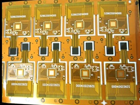
The continuous development of electronic devices and the need for smaller, less-weight, and more compact designs are lead to the creation of flex PCB panels. These panels are created with flexible materials that allow for three-dimensional flexibility, making them best for applications where space constraints and complicated form factors exist. With their flexibility, flex PCB panels provide different advantages to rigid PCBs, making them the best for different industries.
![flex pcb pannels]()
What is a Flex PCB Panel?
A flex PCB panel, also called a flexible printed circuit board, is a PCB board that is constructed with the use of flexible substrate materials, like polyimide or polyester films. These materials offer the required flexibility, and help PCB to be twisted, bent, or folded without compromising its electrical integrity. The flex PCB panel has conductive traces and pads that interconnect electronic components mounted on the board.
Advantages of Flex PCB Panels
Flexibility and Bendability
One of the main advantages of flex PCB panels is their flexibility and bendability features. Unlike rigid boards, which are fixed in structure, these panels can be flexed or bent to fit into tight spaces or conform to complicated form factors. This flexibility is used for more compact and innovative product designs, especially in projects where space is limited.
Space-saving Design
Flex PCB panels enable space-saving designs by eliminating the need for bulky connectors and cables. The flexibility of the PCB itself allows for the direct routing of traces, minimizing the need for additional wiring. This reduction in space requirements can be particularly beneficial in portable electronic devices, where size and weight are critical factors.
Enhanced Durability
They are highly durable due to their flexible manufacturing. Contrary to rigid PCBs, which can be prone to mechanical stress and failures in high-vibration environments, these panels can withstand twisting, bending, and repetitive motion without compromising their functionality. This durability makes them best for applications that needed reliable function under harsh conditions.
Improved Signal Integrity
The flexibility of panels decreases the occurrence of signal interference and impedance mismatches. By allowing traces to be routed directly, the length and complications of signal paths can be reduced, it enhances signal integrity. This benefit is significant for high-frequency and high-speed applications, where signal quality is needed
Cost-effectiveness
While the initial cost of panels can be larger than that of traditional rigid boards, they can provide cost savings in the long run. The reduction of connectors and cables, also reducing the need for additional assembly steps, can cause in lower material and labor expenses. Though, the compact size and less-weight nature of flex panels can lead to savings in shipping and handling costs.
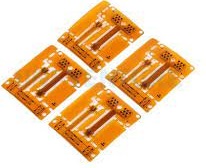
![flex pcb panels]()
Applications of Flex PCB Panels:
[adinserter block="5"]
Consumer Electronics
In consumer electronics, like tablets, smartphones, wearables, and portable gaming devices, flex panels are used to accommodate the slim and compact designs required by consumers. They are used for the seamless integration of electronic components, like displays, touch sensors, and batteries, in space-constrained modules
Automotive Industry
The automotive industry uses these panels...
Read more -
What are the Steps Flexible PCB Manufacturing Process
06/20/2023 at 12:23 • 0 commentsHello readers welcome to the new post. In this post, we will learn What are the Steps Flexible PCB Manufacturing Process. Flexible Printed Circuit Boards are very popular due to their features to provide good flexibility and reliability in different electronic applications. They provide many advantages over rigid PCBs, like enhanced space utilization, good reliability, and increased design flexibility. In this post, we will learn different factors for the flexible PCB manufacturing process. So let's get started with Flexible PCB Manufacturing Process
Introduction to Flex PCB
Flexible PCBs, also called flex circuits or flex boards, are electronic interconnects that can twist, bend, and fold without having an effect on their functionality. They have a thin, flexible substrate created by polyimide or polyester, which helps them to conform to complicated structures and fit into tight spaces. Flex circuit manufacturing comes with different steps, ensuring the manufacturing of high-quality, reliable boards.
[adinserter block="3"]
Understanding Flexible PCBs
Before going to discuss flexible pcb manufacturing, let's discuss the fundamental parameters of flexible PCBs. These circuit boards have 3 main layers: the substrate, conductive traces, and protective cover layers. The substrate work as the base and offers flexibility, while the conductive traces, created with copper, establish electrical connections between components. The protective cover layers protect the traces and make sure durability.
Benefits of Flexible PCBs
Flexible boards provide many advantages that make them best for various industries. Firstly, their flexibility is used for seamless integration into compact and irregularly shaped devices, optimizing space use. 2nd, their less-weight nature decreases the total weight of the electronic assembly. Also, the absence of connectors and the ability to remove complicated wiring harnesses make simple the assembly process, decreasing manufacturing time and costs. Though, the flexibility of these circuits decreases the chances of mechanical failures due to vibrations or shock, and improves overall reliability.
![what is flx pcb]()
Designing a Flexible PCB
Designing a flexible board needed careful consideration of the application's needs, mechanical constraints, and electrical features. It is necessary to select the accurate substrate material, find the number of layers, and define the circuit's layout. The design process consists of optimizing the placement of components, routing traces, and making sure of proper signal integrity. Advanced design software and professional skills in flex circuit design are important to get optimal results.
Steps in the Flexible Printed Circuit Manufacturing Process
![Flexible Printed Circuit Manufacturing Process]()
Step 1: Material Selection
The first step in flexible printed circuit manufacturing is selecting accurate materials. The selection of substrate material is based on parameters like thermal stability, flexibility, dielectric properties, and cost. Polyimide and polyester are commonly used due to their high-temperature resistance, excellent flexibility, and electrical insulation features. The conductive traces are made of copper due to its good electrical conductivity.
Step 2: Circuit Design
After the selection of materials, the next step is circuit design. That makes a schematic diagram of the circuitry, explaining the component placement and determining the routing of traces. The circuit design makes sure optimal electrical performance, signal integrity, and adherence to design rules.
Step 3: PCB Layout
In this step, the circuit design is converted into a physical layout. The layout consisting placing components on the flexible substrate and routing the traces to make electrical connections. Attention to detail is important to confirm the accurate alignment of components and reduces signal interference.
Step 4: PCB Printing
After the layout is completed, the PCB board printing process started. Here transferring the circuit...
Read more -
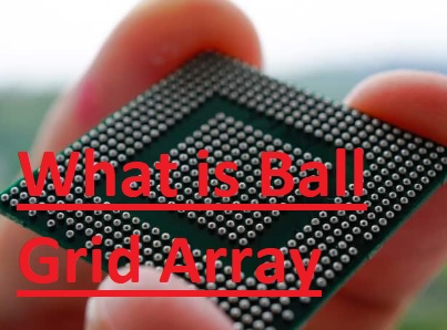
What is Ball Grid Array (BGA) on a PCB Board
06/20/2023 at 12:10 • 0 commentsHi, guys welcome to the new post. In this post, we will discuss What is Ball Grid Array (BGA) on a PCB Board. Ball Grid Array (BGA) is a packaging technology commonly used in electronic circuit boards that have different advantages than other traditional packaging techniques. It is popular due to its ability to accommodate larger interconnections in a small area, so it is best for high-density applications. In this post, we will learn Ball Grid Array (BGA), and other parameters. So let's get started What is Ball Grid Array (BGA)
What is BGA?
- BGA is a surface-mount packaging type where solder balls are configured in a grid-like pattern on the bottom of a component. These solder balls create electrical connections between components and the PCB board. BGA packages are the main part of microprocessors, integrated circuits, and other complicated electronic components.
[adinserter block="3"]
![What is Ball Grid Array]()
BGA vs. Other Packaging Technologies:
Feature BGA PGA LGA Package type Ball grid array Pin grid array Land grid array IC connection Solder balls Pins Solder balls Package size Compact Larger Larger Heat dissipation Good Fair Good Cost expensive Less costly Less costly Complexity More complicated Less complicated Less complicated Applications High-performance devices, devices with a lot of ICs thin devices, General-purpose devices, devices that do not need high performance General-purpose devices, devices that do not need high performance Advantages of BGA:
BGA has different advantages that make it the best for different PCB designs. Firstly, the small size package size allows for more components to be connected on the PCB, leading to higher functionality in a small area. 2nd, the shorter electrical paths between the component and the board improve signal integrity. BGA's thermal features also enable efficient heat dissipation, so they are good for high-power applications.
BGA Assembly Process:
The BGA assembly has different steps. It started with the application of solder paste on the board, followed by component placement with the use of automated machines. The PCB board then passes reflow soldering, where the solder balls melt and make reliable electrical connections. After cooling, the PCB board undergoes inspection to make sure proper alignment and solder joint quality.
Challenges in BGA Assembly:
BGA assembly also has unique challenges. The Main is the accurate alignment of the BGA component due to the absence of leads. BGA components also needed accurate control of the reflow soldering process to avoid problems like solder bridging and voids. With that, the inspection of hidden solder joints and the detection of defects pose additional problems
BGA Inspection and Testing:
Various inspection and testing techniques are employed to make sure the quality and reliability of BGA components. X-ray inspection is used to find hidden solder joints, while optical inspection systems can find defects on the component surface. With that, electrical testing, like ball shear, and ball pull tests, are done to assess the mechanical strength of the solder joints.
BGA Rework and Repair:
For faulty BGA components, rework and repair methods are employed. BGA rework does removing the defective component, cleaning the site, and replacing them with new ones. This process needs advanced tools and skilled operators to avoid damage to the board and adjacent components.
[adinserter block="5"]
BGA Reliability:
BGA packages provide high reliability due to their robust electrical and thermal connections. Though, some factors like mechanical stress temperature cycling, , and aging can affect their long-term performance. Accurate design considerations, material selection, and assembly methods are used to ensure the reliability of BGA components.
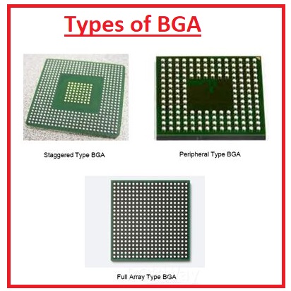
Types of BGA
![Types of BGA]()
1. Ceramic BGA (CBGA):
Ceramic BGA packages are made with the use of ceramic materials and offer excellent thermal properties and high reliability. The ceramic substrate has good heat dissipation,...
Read more -
What is Ball Grid Array (BGA) on a PCB Board
06/20/2023 at 12:06 • 0 commentsHi, guys welcome to the new post. In this post, we will discuss What is Ball Grid Array (BGA) on a PCB Board. Ball Grid Array (BGA) is a packaging technology commonly used in electronic circuit boards that have different advantages than other traditional packaging techniques. It is popular due to its ability to accommodate larger interconnections in a small area, so it is best for high-density applications. In this post, we will learn Ball Grid Array (BGA), and other parameters. So let's get started What is Ball Grid Array (BGA)
What is BGA?
- BGA is a surface-mount packaging type where solder balls are configured in a grid-like pattern on the bottom of a component. These solder balls create electrical connections between components and the PCB board. BGA packages are the main part of microprocessors, integrated circuits, and other complicated electronic components.
[adinserter block="3"]
![What is Ball Grid Array]()
BGA vs. Other Packaging Technologies:
Feature BGA PGA LGA Package type Ball grid array Pin grid array Land grid array IC connection Solder balls Pins Solder balls Package size Compact Larger Larger Heat dissipation Good Fair Good Cost expensive Less costly Less costly Complexity More complicated Less complicated Less complicated Applications High-performance devices, devices with a lot of ICs thin devices, General-purpose devices, devices that do not need high performance General-purpose devices, devices that do not need high performance Advantages of BGA:
BGA has different advantages that make it the best for different PCB designs. Firstly, the small size package size allows for more components to be connected on the PCB, leading to higher functionality in a small area. 2nd, the shorter electrical paths between the component and the board improve signal integrity. BGA's thermal features also enable efficient heat dissipation, so they are good for high-power applications.
BGA Assembly Process:
The BGA assembly has different steps. It started with the application of solder paste on the board, followed by component placement with the use of automated machines. The PCB board then passes reflow soldering, where the solder balls melt and make reliable electrical connections. After cooling, the PCB board undergoes inspection to make sure proper alignment and solder joint quality.
Challenges in BGA Assembly:
BGA assembly also has unique challenges. The Main is the accurate alignment of the BGA component due to the absence of leads. BGA components also needed accurate control of the reflow soldering process to avoid problems like solder bridging and voids. With that, the inspection of hidden solder joints and the detection of defects pose additional problems
BGA Inspection and Testing:
Various inspection and testing techniques are employed to make sure the quality and reliability of BGA components. X-ray inspection is used to find hidden solder joints, while optical inspection systems can find defects on the component surface. With that, electrical testing, like ball shear, and ball pull tests, are done to assess the mechanical strength of the solder joints.
BGA Rework and Repair:
For faulty BGA components, rework and repair methods are employed. BGA rework does removing the defective component, cleaning the site, and replacing them with new ones. This process needs advanced tools and skilled operators to avoid damage to the board and adjacent components.
[adinserter block="5"]
BGA Reliability:
BGA packages provide high reliability due to their robust electrical and thermal connections. Though, some factors like mechanical stress temperature cycling, , and aging can affect their long-term performance. Accurate design considerations, material selection, and assembly methods are used to ensure the reliability of BGA components.
Types of BGA
![Types of BGA]()
1. Ceramic BGA (CBGA):
Ceramic BGA packages are made with the use of ceramic materials and offer excellent thermal properties and high reliability. The ceramic substrate has good heat dissipation,...
Read more -
How to Design a Castellated PCBs Board in 2023
06/20/2023 at 12:00 • 0 commentsHello readers welcome to the new post. In this post, we will discuss How to Design a Castellated PCBs Board in 2023. Designing a printed circuit board needs different considerations to make a successful and reliable electronic product. Castellated PCBs, also called half-holes or plated half-holes, are specialized Pboards with plated edges that helps easy integration into other systems. In this tutorial, we will explore the process of designing a castellated PCB with a board. So let's get started with How to Design a Castellated PCBs Board in 2023
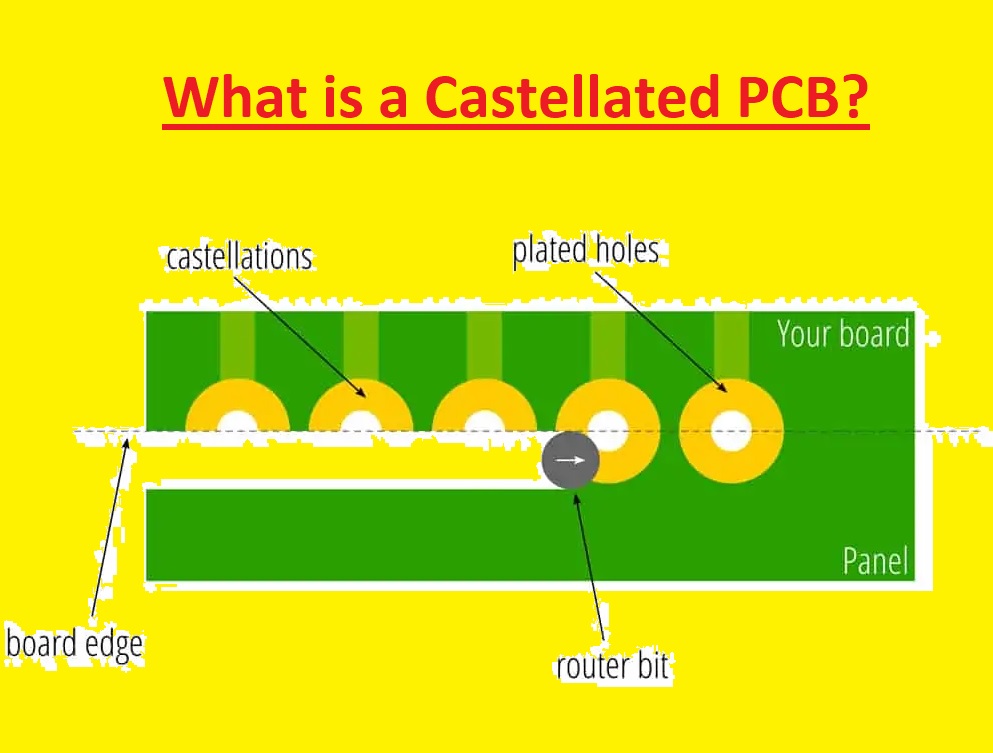
What is a Castellated PCB?
[adinserter block="3"]
A castellated PCB is PCB type that features plated edges on one or more sides. These plated edges normally come with a pattern of half-holes, resembling the battlements of a castle, so they are known as "castellated." These half-holes make easy soldering and mounting of the PCB board onto another board, making them best for applications like module integration or direct attachment to connectors.
![What is a Castellated PCB]()
Benefits of Castellated PCBs
Castellated PCBs have many advantages over traditional PCBs, which are
- Easy integration: The plated edges of castellated boards make simple the integration process with other boards or modules.
- Space-saving: By eliminating the use of separate connectors, castellated boards can save valuable space in electronic assemblies.
- Robust connections: The plated half-holes offer robust and reliable connections, make sure secure solder joints and mechanical strength.
- Design flexibility: Castellated boards provide different versatile placement options, helps designers to optimize space utilization, and accommodate certain application needs
Design Considerations
To design an accurate castellated PCB board, it is necessary to consider these parameters
Step 1: Determine the Purpose
Clearly define the purpose and needs of PCB. Consider factors like required application, size constraints, electrical features, and environmental conditions.
Step 2: Select the Appropriate Software
Select a reliable PCB design software that offers the necessary features for castellated PCB design. Commonly used software areAltium Designer, Eagle, and KiCad.
Step 3: Create the Schematic Design
Make a schematic design that captures the circuit functionality and connectivity. Make sure accurate labeling and documentation of components and connections.
Step 4: PCB Layout
[adinserter block="5"]
convert the schematic design into a physical layout. Carefully place the components, with consideration of power distribution, signal integrity, and thermal management. Follow the best techniques for trace routing and keep a balanced design.
Step 5: Define Castellations
Choose the locations and dimensions of the castellations on the board. Ensure accurate clearance between castellations and other components to prevent short circuits.
Step 6: Verify Design and Manufacture
Perform design rule checks (DRC) and electrical rule checks (ERC) to find and resolve potential faults. Make manufacturing files, like Gerber files, for manufacturing
Step 7: Assembly and Testing
Get services from reliable PCB manufacturers like JLCPCB to ensure accurate manufacturing and assembly of the castellated board. Perform thorough testing to validate the functionality and reliability of the final result
Troubleshooting Tips
While designing castellated boards, you can face some challenges. Here are a few troubleshooting tips explained to overcome common problems
- Make sure proper alignment and solderability of the castellations during the assembly process.
- Verify the compatibility of the castellated board with the target connectors or mating boards.
- Give attention to the mechanical strength and robustness of the castellated edges to handle any potential stress.
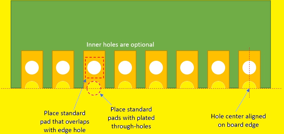
How are castellated pins created on PCB?
![castellated pins]()
Castellated pins, also called castellations or half-holes, are made a PCB board during the manufacturing...
Read more -
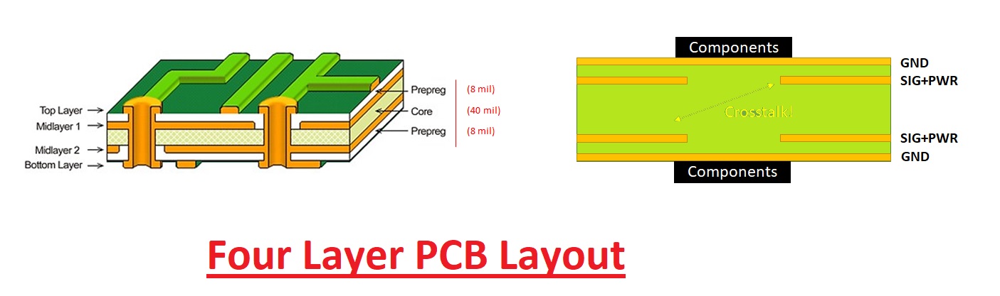
Four Layer PCB Layout: Design Process and Cost of Manufacturing
06/11/2023 at 02:21 • 0 commentsHi, friends welcome to the new post. This post will look at the Four Layer PCB Layout: Design Process and Cost of Manufacturing. Due to its different advantages and benefits, four-layer PCB boards are now the standard for electronic circuit design. This tutorial will cover the four-layer PCB layout design process and manufacturing expenses details. Engineers and PCB designers can make PCBs that are effective and affordable while yet meeting the demands of contemporary electronic devices. so let's get started 4 Layer PCB
What is a 4 layer PCB
- A 4-layer PCB is a printed circuit board that comes with four layers of conductive material separated by insulating layers. It belongs to multi-layer PCB that offers increased flexibility and good performance compared to single-sided or double-sided PCBs.
[adinserter block="3"]
- In these boards, the two outer layers are typically used for component placement and routing of signal traces. These layers can accommodate many components and allow for complicated signal routing. The two inner layers, also called the power and ground planes, offer a solid ground reference and distribute power throughout the circuit.
- The power and ground planes in a 4-layer PCB help to reduce noise and provide a stable power supply to the components. They also help decreases electromagnetic interference by providing a shielding effect. The power and ground planes are interconnected using vias, which helps signals to pass between the layers.
- By having 4 layers, these board PCBs offer improved signal integrity, reduced crosstalk between traces, and better power distribution compared to other boards
![Four Layer PCB Layout]()
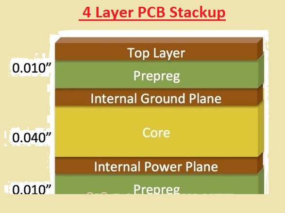
2 Types of 4 Layer PCB Stackup
![4 Layer PCB Stackup]()
There are different types of stack-up configurations for 4-layer PCBs, but two most used are explained here
- Symmetrical Stackup:
Description Signal traces and components Ground plane Power plane Signal traces and components The ground and power planes are configured in the two inner levels of this stack-up. The ground plane work as a barrier against electromagnetic interference and provides a low-impedance return channel for communications. By distributing power uniformly about the circuit, the power plane reduces voltage loss and noise. On the top and bottom layers, signal traces and component placement are done.
[adinserter block="5"]
Asymmetrical Stackup:
Description Signal traces and components Ground plane Power plane Signal traces and components In this stack-up, one of the inner layers is assigned to signal traces and components, while the other internal layer work as a ground plane. The upper layer contains the signal traces and components, while the bottom layer is configured to the power plane. This stack-up allows for controlled impedance routing on the inner layer and provides a solid ground plane for noise reduction.
Benefits of Four-Layer PCB Layout:
Four-layer PCB layouts come with differnt advantages than single-layer and double-layer boards
Improved performance and signal integrity:
Good signal integrity and less noise interference are offered by the additional internal layers of a 4-layer PCB. Performance can be enhanced by designers minimizing crosstalk and maintaining signal integrity by isolating power and ground planes from the signal layers.
Enhanced power distribution:
With separate ground and power planes made possible by these PCBs, the circuit's power distribution is optimized. As a result, voltage loss is reduced, power stability is increased, and noise immunity is enhanced.
Space optimization and compactness:
Designers can get more circuit density and compactness with 4 layers, making it best for devices with a small footprint. The additional layers allow for more effective component routing and placement, which decreases the overall footprint of the board.
Noise reduction and EMI shielding:
The reduction of EMI and improvement of noise immunity are both aided by the separation of the signal layers from the power and ground planes. For high-frequency...
Read more -
The Importance of Copper Pour in Empty Areas on PCBs
06/11/2023 at 02:20 • 0 commentsHello readers welcome to the new post. In this post, we will have a look at The Importance of Copper Pour in Empty Areas on PCBs. Copper pours are important for the design of printed circuit boards. It comes with filling empty areas on the PCB board with copper planes, which provides many benefits for electronic circuits. In this post, we will cover different parameters of f copper pour and its impact on board performance. Let's get started with Introduction to Copper Pour
Introduction to Copper Pour
When designing boards, engineers strive to enhance their functionality, reliability, and performance. The copper pour is a method that helps achieve these goals with the use of the empty areas on the board to enhance its overall performance. By filling these areas with copper planes, engineers effectively manage heat dissipation, decrease electromagnetic interference (EMI), and enhance signal integrity.
[adinserter block="3"]
![Copper Pour on PCBs.]()
What is Copper Pour on PCBs?
Copper pour defines the process of making large areas of continuous copper planes on the circuit board. These planes are attached to the ground or power plane and cover the empty spaces between components and traces. This pour is typically implemented on the internal layers of the board, although it can also be used on the outer layers.
Why is Copper Pour Important?
Enhancing Heat Dissipation
One of the main reasons for incorporating copper pour-in board design is its ability to enhance heat dissipation. The heat produced by active components can be efficiently conducted through the copper planes and distributed about the board. This avoids localized hotspots and makes sure of optimal operating temperatures for components, thereby enhancing their lifespan and reliability.
Reducing Electromagnetic Interference (EMI)
Copper pour also helps to minimize electromagnetic interference within the PCB. The continuous copper planes work as shields, reducing the coupling of electromagnetic fields among traces and components. This decreases the chances of cross-talk, signal degradation, and unwanted noise, resulting in enhanced overall system performance.
Improving Signal Integrity
Another main advantage of the copper pour is its impact on signal integrity. By providing a less-impedance path, the copper planes help smooth signal transmission and decrease the effects of impedance mismatch. This is important for high-speed digital and analog circuits where maintaining signal integrity is required.
Wholesale PCBs SMT Stencil & PCBA Service Provider Special offer:$2 for 1-8 layer PCBs
Copper Pour Design Considerations
To make effective copper pour implementation, certain design considerations must be followed
The copper weight for the pour area is based on the certain needs of the board design. High copper weights can offer good heat dissipation and current-carrying capacity, but they can also increase manufacturing expenses and introduce etching challenges. It is necessary to balance these factors and choose a good copper weight that aligns with the design goals.
Clearance and Spacing
Clearance and spacing about the copper pour area are critical to avoid unintended shorts or signal interference. Proper clearances must be maintained between the copper pour and other components, and signal lines. and traces, Adhering to design guidelines and industry standards make sure reliable performance and prevents potential issues.
Shape and Placement
The shape and placement of the copper pour areas must be carefully considered to optimize the board performance. Irregular or poorly placed copper pour can cause uneven heat distribution or ineffective EMI shielding. Engineers must strive for a well-planned copper pour design that enhances benefits while minimizing potential failures
Split Planes
In some conditions, it can be necessary to split copper pour areas into many sections or planes. This is used for good control of current flow, decreased impedance, and improved...
Read more -
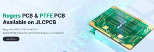
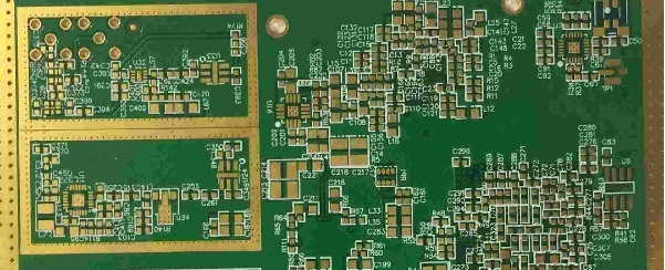
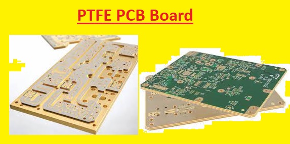
PTFE PCBs: The Ultimate Solution for High-Frequency Applications
04/15/2023 at 08:56 • 0 commentsPrinted Circuit forums (PCBs) are vital additives in the electronics enterprise. They play a critical function in connecting electronic additives to gadgets, machines, and systems. But, now not all PCBs are created identically. In relation to high-frequency applications, well-known PCBs might not carry out optimally. That is in which PTFE PCBs are available. Here we will cover the details of PTFE PCBs, their capabilities, their benefits, and why they are the ultimate solution for high-frequency programs.
What is PTFE PCB?
- PTFE, or polytetrafluoroethylene, is a type of thermoplastic polymer this is used in different industries due to its superb thermal, electrical, and chemical houses.
- Whilst utilized in PCBs, PTFE can offer superior performance compared to different substances due to its high dielectric regular, low loss tangent, and fantastic thermal stability.
- Making PTFE PCBs involves embedding PTFE fabric into the PCB substrate using a variety of techniques, such as laminating or extruding. A PCB with outstanding electric and thermal performance is the final product, making it a great choice for high-frequency, high-electricity, and high-temperature applications.
PTFE material properties
- There are differnt features of material used for the creation of PTFE listed here
- It provides the good dielectric strength
- It has less value of the dissipation factor
- This material has High thermal stability
- Comes with the feature of chemical resistance
- This material absorbs the less moisture
Features of PTFE PCBs
Due to their distinct qualities, PTFE PCBs are ideal for high-frequency applications. These qualities consist of:
Low dielectric constant
Due of its low dielectric constant, it can efficiently store electrical energy. In high-frequency applications, where signal loss can be considerable, this characteristic is crucial.
Low loss tangent
This board has a low-loss tangent, which means it can dissipate electrical energy with minimal loss. In high-frequency applications, where signal loss can reduce system performance, this feature is essential.
High thermal stability
Because of its great thermal stability, PTFE can resist extreme temperatures without deteriorating. This characteristic is crucial in high-frequency applications where system performance might be impacted by temperature variations.
Chemical resistance
As These boards are resistant to the majority of chemicals, it may be used in extreme settings where regular PCBs would not hold up.
Low moisture absorption
It is the perfect material for high-humidity conditions because of its low moisture absorption, which means it can withstand moisture infiltration.
PTFE PCBs from JLCPCB
![roger jlcpcb]()
- Leading suppliers and producers of PTFE PCBs are JLCPCB. With years of PCB industry expertise, JLCPCB has been a reliable partner for clients all over the world.
- To accommodate the various requirements of its clients, JLCPCB provides a variety of PTFE PCB choices. JLCPCB has the knowledge and capacity to provide high-quality PTFE PCBs, regardless of whether you want a straightforward single-layer PCB or a complicated multi-layer PCB.
- The cutting-edge production capabilities of JLCPCB are one of the main benefits of hiring them for your PTFE PCB needs.
- JLCPCB makes use of cutting-edge tools and production...
-
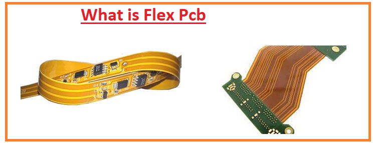
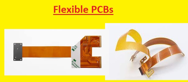
Flexible PCBs: The Future of Electronics Manufacturing
04/15/2023 at 08:55 • 0 commentsDue to their numerous benefits over conventional rigid PCBs, flexible printed circuit boards (PCBs) have experienced a substantial shift in the electronics industry in recent years. The increasing use of these PCBs in different types of industries, like automobile, healthcare devices, aviation, and consumer electronics, is a result of the desire for small size, less weight, and flex electronic devices. The fundamentals of flexible PCBs, as well as their advantages, uses, methods of production, and potential trends, will all be covered in this article.
Introduction
Flexible PCBs sometimes referred to as flex circuits or flexible circuits, are a creative solution that offers electronic devices a great level of design freedom and dependability. These boards are created through the use of substrate material like polyimide, which can be easily bent, twisted, or folded into a different structure without losing its functionality, as opposed to rigid PCBs, which are comprised of the solid substrate material.
What are Flexible PCBs?
Electronic circuits are printed on flexible substrates called flexible PCBs, which are typically polymer films like polyester or polyimide. These circuits are constructed from numerous layers of conductive traces that are printed using a specialized technique onto the flexible substrate material. The conductive traces link numerous parts, including resistors, capacitors, and transistors, which are surface-mounted onto the flexible substrate (SMT).
![jlcpcb flexible pcb Flexible PCBs]()
Flexible PCB Benefits
- There are different advantages of this board explained here
1. Space-saving
- These PCB boards may be curved to meet the curvature of the device and can be engineered to fit into small areas, conserving important space.
2. Weight reduction
- These boards are lightweight compared to standard rigid PCBs, making them excellent for applications where weight is a vital element.
3. Increased Reliability
- As flexible boards contain fewer interconnects than conventional rigid PCBs, the likelihood of failure from soldering, vibration, or heat stress is lower.
4. Design Flexibility
- These type of PCBs enable designers to develop custom-shaped circuits that perfectly suit certain applications since they can be molded into a variety of forms and sizes.
5. Cost-Effective
- Since they lower the number of interconnects and do not require connections, flexible PCBs are more affordable than rigid ones.
Flexible PCB Applications
- There are differnt types of applications of these boards listed here
1. Consumer Electronics
- Consumer devices such as smartphones, tablets, and wearables require this PCB. To fit into small form factors, these devices need flexible circuits that can be folded or twisted.
2. Automotive
- In the automobile sector, flexible boards are utilized for things like dashboard displays, lighting, and engine control modules. Flexible PCBs are more flexible and reliable, which makes them perfect for the challenging automobile environment.
3. Aerospace
- In the aerospace sector, flex PCbs are utilized for satellite systems, avionics, and communication systems, among other things. These circuits are perfect for space and aircraft applications due to their excellent dependability, lightweight, and flexibility.
4. Healthcare
- In the medical industry, flexible PCBs are utilized in wearable health monitoring, diagnostic devices, and medical imaging.
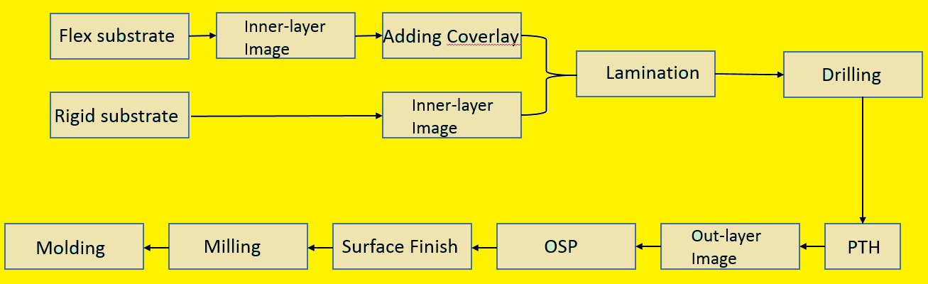
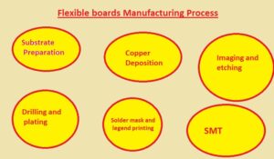
Flexible boards Manufacturing Process
![Flexible boards Manufacturing Process jlcpcb flexible pcb Flexible PCBs]()
- Flexible PCB fabrication requires a number of stages, including:
1. Substrate preparation
The substrate material must first be ready, which is often a polymer sheet like polyimide. In order to assist the electrical traces adhering to the substrate, the substrate is cleaned and covered with an adhesive substance layer.
2. Copper deposition
- The second stage involves utilizing an electroless copper plating technique to apply a thin coating of copper to the substrate. The conductive lines connecting the different components are formed by the copper...
-
Roger Material: The Ultimate Solution for High-Speed and High-Frequency PCBs
04/15/2023 at 08:53 • 0 commentsBecause to its distinct qualities, Rogers PCB is a type of printed circuit board that is frequently utilized in the electronics industry. This article will discuss Rogers’s PCB, including its characteristics, benefits, manufacturing issues, and applications.
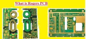
What is Rogers PCB?
- A printed circuit board known as a Rogers PCB employs Rogers material as its primary substrate.
- A high-frequency laminate known as the Rogers material is made of a combination of glass, ceramic, and polymer components.
- This substance is well-known for having a low-loss tangent and dielectric constant, which makes it the best option for high-frequency and high-speed applications.
![rogers pcb]()
Properties of Rogers PCB
- Here different features of Rogers board explained
Dielectric constant
- Since Rogers PCB has a low dielectric constant, high-frequency signals can be supported without degradation. Rogers PCB’s dielectric constant can range from 2.2 to 10.2.
Loss tangent
- This pcb board has a low-loss tangent, high-frequency signals may be sent there without being attenuated. The value of loss tangent might be anywhere from 0.0009 and 0.0040 for this board.
Thermal conductivity
- The excellent thermal conductivity of these PCBs allows for effective heat dissipation. The value of thermal conductivity can range from 0.4 to 1.4 W/mK.
Glass transition temperature
- As Rogers PCB has a high glass transition temperature, it can endure high temperatures without warping or being damaged. The value of glass transition temperature might be anywhere between 150 and 280 °C.
Tensile strength
- This board comes with a high tensile strength, it can endure mechanical force without cracking. Its tensile strength range of 70 to 130 MPa.
Moisture absorption
- It comes with a low moisture absorption rate, which implies that it can withstand moisture and humidity. Between 0.01 and 0.09% of Rogers PCB can absorb moisture.
Advantages of Rogers PCB
- There are differnt advantages provided by this board explained here
High-frequency and high-speed applications
- It has a low dielectric constant and loss tangent making it perfect for high-frequency and high-speed applications.
Low signal loss and low noise
- High signal integrity and reliability are achieved because of these board has features to transfer high-frequency signals with little attenuation and noise.
Good thermal management
- Because to the excellent thermal conductivity of Rogers PCB, it can dissipate heat effectively, enhancing reliability and endurance.
High dimensional stability
- It has better reliability and precision because to its ability to keep its form and size at high temperatures and mechanical stress..
Good chemical resistance
- Rogers PCB has increased dependability and lifespan since it can withstand chemical and environmental harm.
Rogers PCB Applications
- The main applications of Rogers PCB are explained here
Telecommunications and wireless devices
- Antennas, transmitters, receivers, and filters are common examples of wireless and telecommunications equipment that frequently employ Rogers’s PCB.
Aerospace and defense industry
- Applications including radar systems, satellite communication, and missile guidance systems all employ Rogers PCB in the aerospace and military sector.
Medical devices
- Medical devices such as pacemakers, MRI scanners, and ultrasound machines all make use of Rogers’s PCB.
Automotive industry
- For purposes including GPS systems, engine control units, and sensors, the car sector uses these boards
Consumer electronics
- In different consumer electronics for example smartphones, tablets, and laptops, Rogers PCB is used for Wi-Fi, Bluetooth, and NFC applications.
Challenges in Manufacturing Rogers PCB
- There are some challenges faced by te ROgers board during their construction that are explained here
Cost
- Due to the high cost of the Rogers material and the manufacturing process, these boards more expensive than conventional FR-4 PCB. Specialized tools...
-
Roger Material: The Ultimate Solution for High-Speed and High-Frequency PCBs
04/15/2023 at 08:47 • 0 commentsBecause to its distinct qualities, Rogers PCB is a type of printed circuit board that is frequently utilized in the electronics industry. This article will discuss Rogers’s PCB, including its characteristics, benefits, manufacturing issues, and applications.
What is Rogers PCB?
- A printed circuit board known as a Rogers PCB employs Rogers material as its primary substrate.
- A high-frequency laminate known as the Rogers material is made of a combination of glass, ceramic, and polymer components.
- This substance is well-known for having a low-loss tangent and dielectric constant, which makes it the best option for high-frequency and high-speed applications.
![rogers pcb]()
Properties of Rogers PCB
- Here different features of Rogers board explained
Dielectric constant
- Since Rogers PCB has a low dielectric constant, high-frequency signals can be supported without degradation. Rogers PCB’s dielectric constant can range from 2.2 to 10.2.
Loss tangent
- This pcb board has a low-loss tangent, high-frequency signals may be sent there without being attenuated. The value of loss tangent might be anywhere from 0.0009 and 0.0040 for this board.
Thermal conductivity
- The excellent thermal conductivity of these PCBs allows for effective heat dissipation. The value of thermal conductivity can range from 0.4 to 1.4 W/mK.
Glass transition temperature
- As Rogers PCB has a high glass transition temperature, it can endure high temperatures without warping or being damaged. The value of glass transition temperature might be anywhere between 150 and 280 °C.
Tensile strength
- This board comes with a high tensile strength, it can endure mechanical force without cracking. Its tensile strength range of 70 to 130 MPa.
Moisture absorption
- It comes with a low moisture absorption rate, which implies that it can withstand moisture and humidity. Between 0.01 and 0.09% of Rogers PCB can absorb moisture.
Advantages of Rogers PCB
- There are differnt advantages provided by this board explained here
High-frequency and high-speed applications
- It has a low dielectric constant and loss tangent making it perfect for high-frequency and high-speed applications.
Low signal loss and low noise
- High signal integrity and reliability are achieved because of these board has features to transfer high-frequency signals with little attenuation and noise.
Good thermal management
- Because to the excellent thermal conductivity of Rogers PCB, it can dissipate heat effectively, enhancing reliability and endurance.
High dimensional stability
- It has better reliability and precision because to its ability to keep its form and size at high temperatures and mechanical stress..
Good chemical resistance
- Rogers PCB has increased dependability and lifespan since it can withstand chemical and environmental harm.
Rogers PCB Applications
- The main applications of Rogers PCB are explained here
Telecommunications and wireless devices
- Antennas, transmitters, receivers, and filters are common examples of wireless and telecommunications equipment that frequently employ Rogers’s PCB.
Aerospace and defense industry
- Applications including radar systems, satellite communication, and missile guidance systems all employ Rogers PCB in the aerospace and military sector.
Medical devices
- Medical devices such as pacemakers, MRI scanners, and ultrasound machines all make use of Rogers’s PCB.
Automotive industry
- For purposes including GPS systems, engine control units, and sensors, the car sector uses these boards
Consumer electronics
- In different consumer electronics for example smartphones, tablets, and laptops, Rogers PCB is used for Wi-Fi, Bluetooth, and NFC applications.
Challenges in Manufacturing Rogers PCB
- There are some challenges faced by te ROgers board during their construction that are explained here
Cost
- Due to the high cost of the Rogers material and the manufacturing process, these boards more expensive than conventional FR-4 PCB. Specialized tools...
-
Rogers PCB & PTFE PCB: High Frequency PCB is available on JLCPCB
03/15/2023 at 12:58 • 0 commentsHello, readers welcome to the new post. In this post we will discuss Rogers PCB & PTFE PCB: High Frequency PCB is available on JLCPCB. the high-frequency board is the best option for projects like signal transmission among two differnt devices. This PCB board uses certain types of materials for attaining high frequency. As compared to other normal PCB boards high frequency boards produce small but high-frequency signal impedance. These boards are considered as the main part of products where certain signals are required. It operates for five hundred megahertz to two GIGa Herts frequency ranges. So it is a significant part of high-speed signal transmission projects
To ensure the quality of boards there are different tests are performed such as AOI, E-testing, X-RAY, impedance control, high temperature, and high humidity, etc. FR4, high TG FR4, Roger PCB, high-frequency material, and metallic-based board are commonly used in electronic projects. Here JLCPCB has introduced its High-frequency services for their clines with great quality and reasonable prices. Details are explained below. So let’s get started
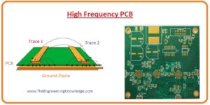
What is High Frequency PCB
- if you are working on a wireless system or related application that has to transmit the signal between points then the best option is to use the high-frequency PCB. The frequency for these boars are 500 megahertz to two Gigahertz.
- They are the finest option for different applications like high-speed designs microwaves phones and some other electronic projects
- These boards are sensitive so it uses high-frequency laminates to maintain the heat transfer during operation
- With the boards used in our project of high-frequency type decide the operation of our project signal. The change in the dielectric constant of the material has an impact on the impedance of baord
![hf pcb]()
Features of high frequency circuit board
- Here are some features of high frequency that are explained.
- It is smaller and more stable there is no delay in signal transmission provided by these baord and the finest option of signal transmission. It has the ability to decrease signal wastes and cooper free foil separates with temperature variation.
- These boards have some features like impact resistance heat resistance, peel resistance, and chemical resistance. With that high peel, resistance enhances the signal quality of the board
high-frequency circuit boards Materials
- As these boards operate on high-frequency values so they are affected by the high temperatures conditions.
- If the material used for these boards is not good it can cause thermal stress accumulation. so must use such material having a good coefficient of thermal expansion. With that material must have a high value of stability. That will work for a long duration
- The material used for these board construction has high conductivity and electrical conductivity
- As HF boards are used in harsh environments so must have high corrosion resistance and moisture resistance. That is why the material used must be moisture-proof. High-frequency signals are sensitive to noise.
- So there must be the material used that has good impedance tolerance for HF board construction
![hf features]()
Rogers PCB & PTFE PCB: High Frequency PCB is available on JLCPCB
![roger jlcpcb]()
- JLCPCB is the best PCB supplier that is Established in 2006, JLCPCB is at the forefront of the PCB industry. With more than 15 years of continuous innovation and improvement based on customer needs, they have grown rapidly to become the world’s leading PCB manufacturer, providing rapid production of highly reliable and cost-effective PCBs and creating the best customer experience in the industry. JLCPCB is constantly striving to be more efficient and reduce costs. They promise to offer customers the most economical PCBs forever. JLCPCB produces the cheapest yet high-quality printed circuit boards, probably due to economies of scale, extremely high production efficiency, and lower labor costs.
- In the recent past, JLCPCB received a lot...