 Pavel
Pavel Yann Guidon / YGDES
-
Logic gate parameters
09/15/2017 at 07:11 • 1 commentHaving obtained 50 MHz analogue single channel oscilloscope opened new avenues for researching of electronics. Here I will present the results regarding measurements of logic gate parameters.
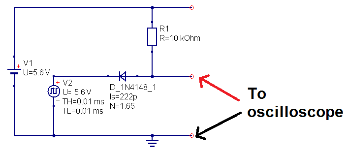
I started with the most basic "gate", made up from one diode and one resistor. This is diode logic gate AND with only one input, something like buffer. Here is the schematics:
![]()
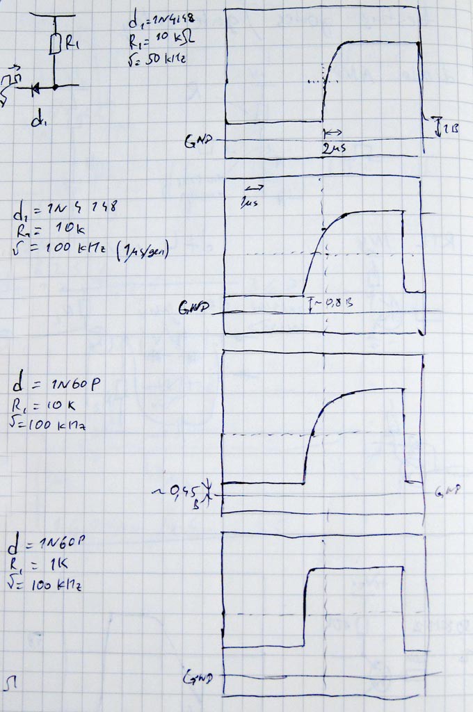
As I looked at slope of the rising edge, it became apparent, that it is depended on the value of resistor used. The less resistance, the more steep edge ensures (following are my drawings from oscilloscope screen; 1n60p is Schottky diode):
![]()
This circuit is used as input stage in my gates, so getting fast response from it is essential. On the other hand, it is curious for me, as I had read that diode has very little capacitance and can switch to and from conduction in matter of picoseconds. Somehow it seems that it does so only when switching from noncunduction to conduction. For it to stop conducting it needs some time, as though there is a need for some charge to be pumped? The more current flows through it, the more readily it ceases to conduct, it seems. By the way, using Shottky diode instead of regular one made no apparent change.
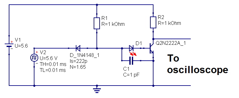
Anyway, proceeding to proper gate, the DTL inverter:
![]()
The schematic shows the one I came up with, which is the best for its speed (has delay somewhere near 175 ns).
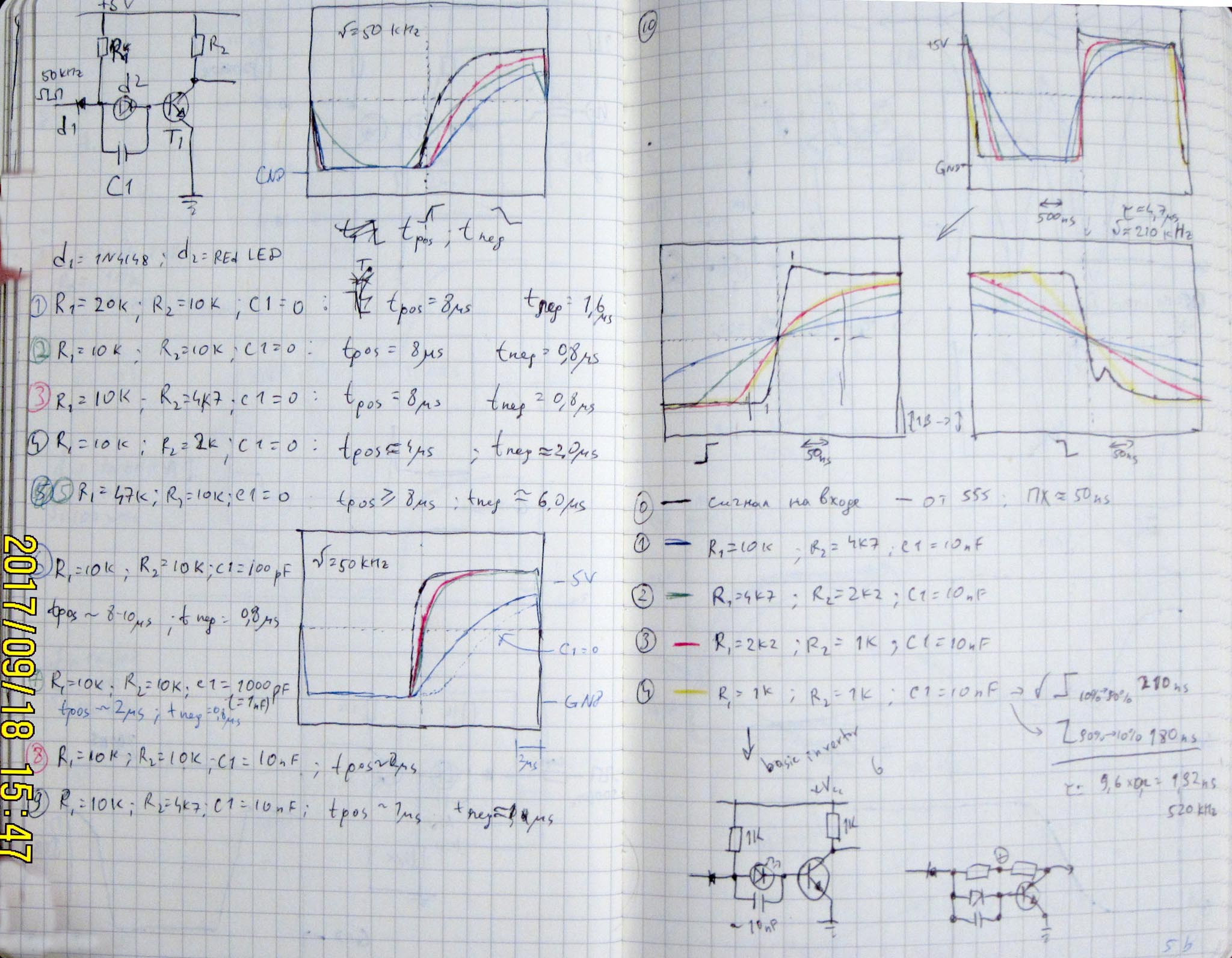
Here is account regarding search for right combination of resistances and capacitance:
![]()
Square wave signal of nearly 50 kHz is generated by 555 IC, it have nice edges with rise and fall times less that 50 nanoseconds. On graphs on the right page it represented by solid black line. As one can see, adding capacitor makes for much faster response of transistor -- it switches off much faster. Also lowering resistor values makes for sharper edges in general (lowering R1 makes falling edge sharper, and lowering R2 makes rising edge sharper).
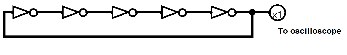
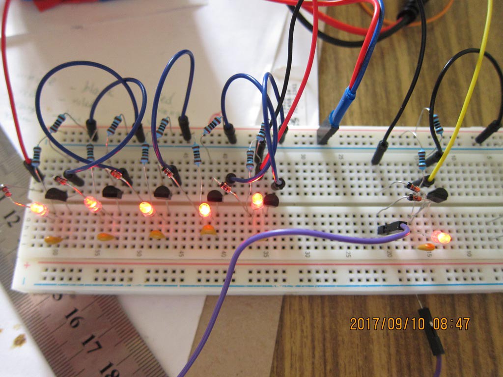
For measuring gate delay I used chain of 5 inverters with output from 5th fed to input of first one. From there also tapped signal to oscilloscope. That way I had free oscillations with period = 10*delay time.
![]()
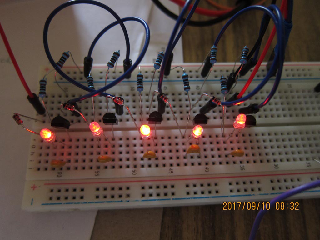
Here is the picture of such setup:
![]()
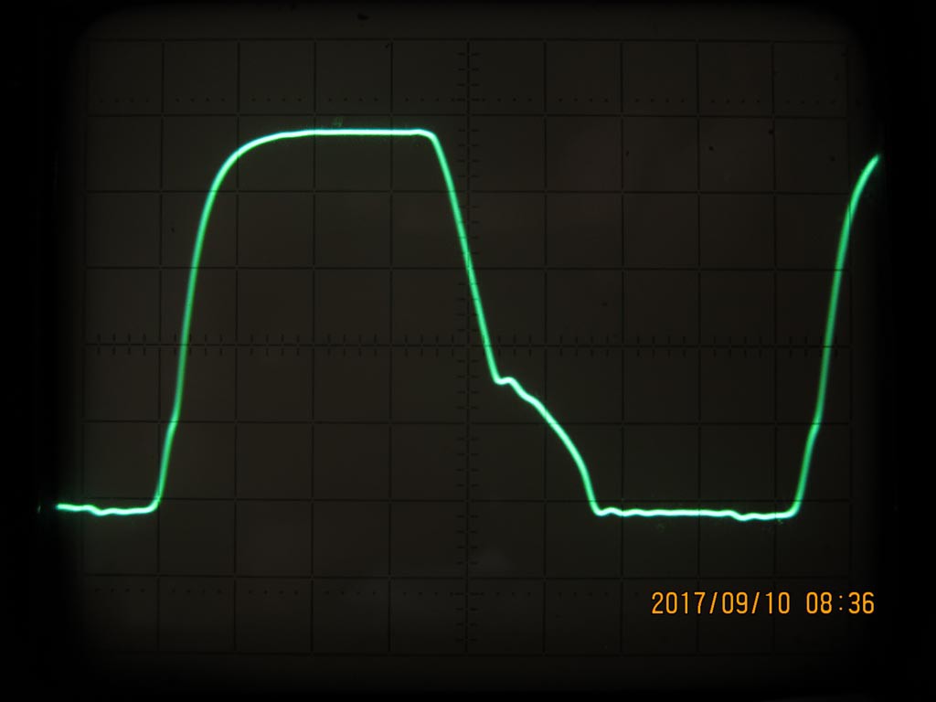
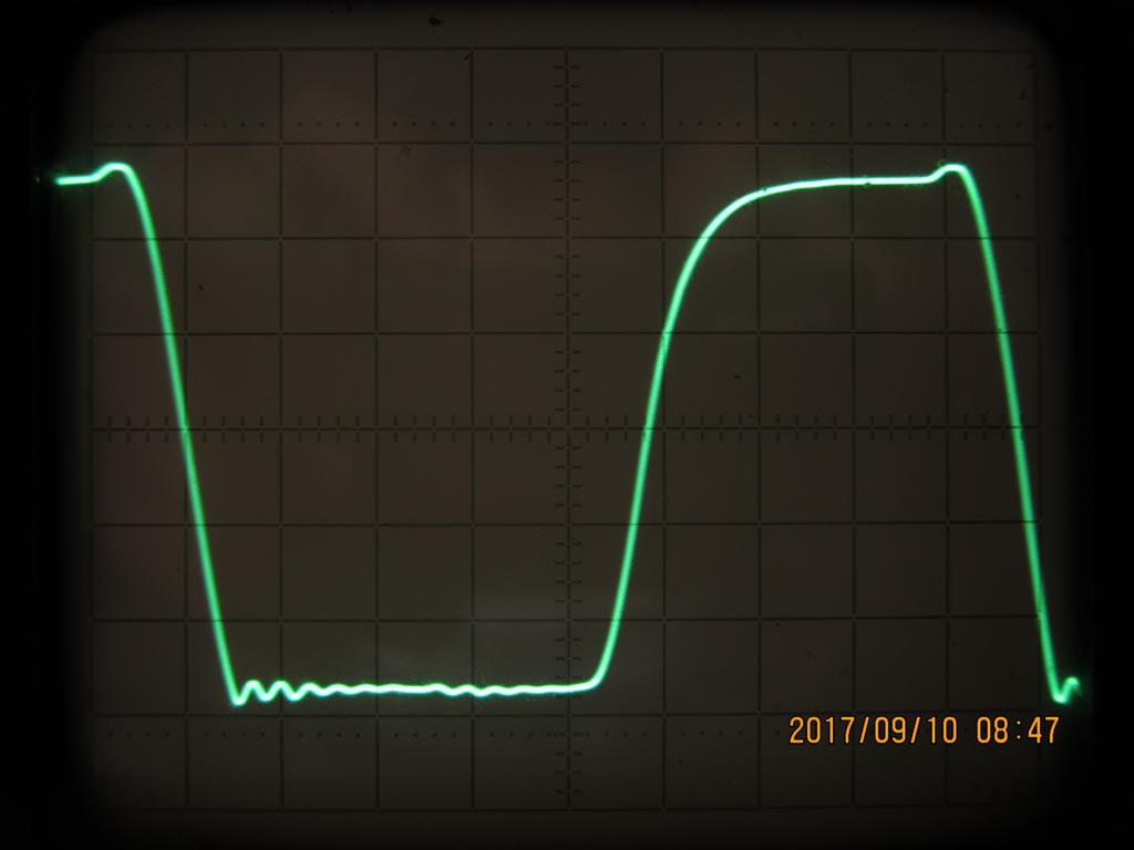
And this is the trace on oscilloscope screen (reticule: one cell horizontally = 200ns, verically = 1 Volt):
![]()
As one can see, falling edge of output from gate, when loaded by the next gate becomes slower after it falls below certain level (1.95 V above ground) which coincides by LED's drop. Why is it so? When gate is not loaded, or loaded by simple resistance to ground, the falling edge is featureless:
![]()
![]()
![]()
By the way, adding resistor from base of transistor to ground have not yielded good result -- while it makes rising edge slightly sharper, the falling edge quite noticeably becomes less sharp.
Also I tried to use capacitors in parallel to input diodes, and another time replaced input diode with transistor -- while there was some improvement in delay time (it became as little as 125 ns) and I was able to use higher resistance at input, there was drawback, in my opinion: while gate was loaded by another gate (like in invertor chain), HIGH signal had been lowered almost to a half value of positive rail. By the way, when measuring unloaded signal (like in the last series of pictures), output signal had full swing from rail to rail. Why? I am personally at loss here.
-
Flea market
09/02/2017 at 14:23 • 0 commentsRecently I discovered for myself that our local flea market have many interesting items to offer, and for prices that are very satisfying. For example in the course of last week I acquired old little black and white crt tv for experimenting, just for 3 USD, and, more valuable item, analog oscilloscope with bandwidth of 50 MHz for just 60 USD, which I suppose is a very good bargain. These items are in excellent working condition despite being some 25-30 years old (of Soviet manufacture). These acquisitions will much improve my quest for understanding electronics, I hope. Certainly, the oscilloscope will much help with study of logic gate delays and thus with improvement of gate performance.
-
Thoughts #2
07/06/2017 at 09:28 • 0 commentsI figured it will take 37 different parts to build one memory cell (complete with three-state output), and one 16 bit register will require up to 600 parts to solder, and I see it will be a hell of work and time to solder it together and make it work properly, so the registers for display will definitely be repurposed if I will build a CPU.
The memory cell consists of data latch with additional ~set and ~reset inputs and tri-state output stage. The latch is made of 2 2NAND and 2 3NAND dtl gates, each of which have three resistors, one LED, one transistor and number of diodes equal to number of inputs as their constituent parts. The tri-state output stage is made of 5 npn transistors and two resistors.
This user joined on 04/10/2017.
My Projects
My Pages
Projects I Like & Follow
 Alastair Hewitt
 Dr. Cockroach
 Igor
Igor Martian
 John Lonergan
 Charlie Smith
 Ced
Ced David Boucher
 Dmitry
 Mitsuru Yamada
 matseng
 kaimac
 Tim Wilkinson
 Robert Gill
 Augusto Baffa
 Jacob Christ
Share this profile
ShareBits


Thank you for liking my #CRISS CP/M 8-bit Homebrew DIY Computer (AVR based) project! Join us at https://discord.gg/cbtxAJE2

Hi @Pavel, thank you for following my #Homebrew CPU list.

I like your display of transistor projects. It is inspiring! Also, it makes discrete logic feel more approachable. As I want to make NMOS and CMOS circuits more than RTL or TTL, I may now order a bunch of mosfets from digikey on my next order :)

Good afternoon Pavel and thank you for the follow and like for my Cardboard Computer project :-)
Thank you for liking my #Prehistory of my homemade PERSEUS computers ! When I think back to my 40 years ago, I was able to make some hardware, but I was not able to make anything equivalent to system software. In a recent project, I overcame this problem and was able to use a home-made floating-point interpreter to calculate the position of a planet from its orbital elements, but it was a very long road.