A while ago I needed a quick and dirty way to see what's going on in a clocked down design of mine and found myself with no appropriate tools around (and I was like "oh, shift / carp, digging into something as simple as this with an MSO / logic analyzer is an overkill"). Few hours into it and the "blinker" was born.
The design is straightforward - row scanner (driving low side NMOS current sinks) and column current sources (FPGA I/O cells in this case). On each clock cycle one of the R_i lines is asserted, the corresponding NMOS transistor is switched on and starts sinking current to the ground, while the C0-C7 lines are wired to the byte to be displayed, or, like in ((logic cell)register_bit[j]→(I/O cell)C_j)→[220R]→LED(c_j⇥⎯r_i)→NMOS_sink_i→GND. The value of 220R was chosen so that the column wouldn't draw more that 5-6mA pulsed current from the FPGA I/O cell. The selected NMOS transistors are capable of handling 8x6mA safely, so this shouldn't be a problem. The general formula is R_limit = (Vcc - Vled - Vds_drop) / I_led. One may ignore the drop term for simplicity, it will lower the max current figure a li'l bit, but it's OK).
If you need more current / higher Vcc, you must use a high side driver as well, which usually is implemented with an NMOS-PMOS pair (or NPN-PMOS, but I'd rather stay away from logic + BJTs). PMOS transistors are inverse logic devices (logic 1 means off) so a second NMOS or NPN transistor is added, acting like an inverter. It also isolates the logic output should the high side driver is sourcing current at a voltage level higher than Vcc. You may want to read AN804 / Vishay Siliconix. The overall picture changes to (((logic cell)register_bit[j]→(I/O cell)C_j)→NMOS_inverter_j→(Vcc→PMOS_source_j))→[RRR]→LED(c_j⇥⎯r_i)→NMOS_sink_i→GND.
While you may skip the bypass caps (step 4, 2x100n, 2x10u) if you go low side only (stop at step 10), having both drivers requires a "good" bypassing (as good as it gets on a protoboard), you'll be pulsing the Vcc rail after all.
Follow the building steps. Once your board is ready, test it. Connect the Vcc/GND to a 3.3V PSU (or a 3V battery pack). Nothing should be lit, there should be no current flowing (use a DVM set to a mA range). Now connect all of the columns C to Vcc, the matrix should still be dark, no current. Proceed by asserting the individual R lines and you should see a lit row of LEDs (less than 50-60mA on the meter). This pretty much ensures there're no shorts / blown FETs / bad solder joints etc. This test is also good for the C' pins.
You're now ready to connect your blinker to the EB85. Go for the I/O pins of the J4 header (it also has 3.3V pins on it and is close to the edge of the EB). Use jumper wires and connect the GND, R0-R7 and C0-C7 / GND, Vcc, R0-R7 and C'0-C'7 (but never both C and C' pins at the same time, if you also soldered the high side driver). Don't use the J3 pin (pin 22) as it's connected to the 12MHz oscillator.
Now go to latticesemi.com and download iCEcube2 and Diamond Programmer. Set the jumpers on your EB85 so that you'll be programming the CRAM over USB (or the serial flash if you want). Fire the iCEcube, create a new project and copy-paste the Verilog code (matrixdriver.v. You'll have to define a PCF with CLK input set to J3 and rows[0]...rows[7] and columns[0]...columns[7] set to the I/O pins you have just chosen. Consult with the iCEcube manual. If everything is OK you'll see the 64bit LFSR pattern from the Xilinx XAPP052 flashing, shifting right every ~90ms (~11Hz). Enjoy!
My "blinker" in action: https://drive.google.com/open?id=16Qq6392cpr6KxDlNpSg93MblcJA2zQ8b
Sure enough, you may also display hexadecimal numbers with this driver, you only have to upload a different Verilog design (segdriver.v) and connect the rx/cx pins in a slightly...
Read more »
 tomcircuit
 Ted Yapo
 John Lonergan
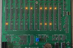
 Joe Wingbermuehle