ZX80/ZX81 remakes
“Sinclair video generation is like a dog's walking on his hind legs. It is not done well; but you are surprised to find it done at all.”
“Sinclair video generation is like a dog's walking on his hind legs. It is not done well; but you are surprised to find it done at all.”
To make the experience fit your profile, pick a username and tell us what interests you.
We found and based on your interests.
2023-09-02
This is the approach I have decided upon.
This has the following advantages
The memory map should look like this:
/*
RAM onboard:
     a a a a a a a a
     1 1 1 1 1 1
     5 4 3 2 1 0 9 8

00h,02h   0 0 0 0 0 0 x 0     ZX81 RAM patches at 00XXh and 02XXh
0x20      0 0 1 0 0 x x x     G007 RAM (2k space)
0x30      0 0 1 1 0 x x x     Spare RAM

ROM unified:

0x0c      0 0 0 0 1 1 0 0     ZX81 ROM patch
0x28      0 0 1 0 1 x x x     G007 ROM (2k space)
0x38      0 0 1 1 1 x x x     Spare ROM

RAM expansion:

0x40      0 1 0 x x x x x     RAM expansion (8k)
0x40      0 1 x x x x x x     RAM expansion (16k)
0x80      1 x x x x x x x     RAM expansion (above 32k)

Intermediate terms:
*/

RAM_patches            = !a15 & !a14 & !a13 & !a12 & !a11 & !a10 & !a8 ;

ROM_8k_at_0000h        = !a15 & !a14 & !a13 ;

RAM_2k_at_2000h        = !a15 & !a14 &  a13 & !a12 & !a11 ;
ROM_2k_at_2800h        = !a15 & !a14 &  a13 & !a12 &  a11 ;
RAM_2k_at_3000h        = !a15 & !a14 &  a13 &  a12 & !a11 ;
ROM_2k_at_3800h        = !a15 & !a14 &  a13 &  a12 &  a11 ;

/*
The terms above simplify if you wish to minimise logic:
*/

RAM_at_2000h_and_3000h    = !a15 & !a14 &  a13 &        !a11 ;
ROM_at_2800h_and_3800h    = !a15 & !a14 &  a13 &         a11 ;

/*
However I shall leave them unsimplified so they can be modified more easily:
*/

/*
Drive pins:
*/

RAM_expansion        = mreq & a15        // at 8000h, above 32
            + mreq & a14        // at 4000h or C000h

RAM_onboard        = mreq & RAM_2k_at_2000h
            + mreq & RAM_2k_at_3000h;

/*
NB if onboard RAM is 8K or less, then RAM at
00XX and 02XX are aliased at
20XX and 22XX respectively.
If you have more, then they are not,
and the higher addresses are free for your use.
*/

ROM_unified    = mreq & ROM_8k_at_0000h & !(RAM_patches)
        + mreq & ROM_2k_at_2800h
        + mreq & ROM_2k_at_3800h ;

/*
NB the logic above will probably expand to something like:
*/

ROM_unified_alt =
    + mreq & ROM_8k_at_0000h &    a11        // 1000h
    + mreq & ROM_8k_at_0000h &    a10        // 0800h, 1800h
    + mreq & ROM_8k_at_0000h &    a8;        // 0400h, 0600h, 1400h, 1600h

/*
So the memory address decoder uses 9 inputs and 3 outputs

in:    A15...8
    !mreq

out:    ROM_unified
    RAM_onboard
    RAM_expansion

That leaves 10 pins, up to 7 outputs and 3 inputs or 1 output and 9 inputs.
*/

memory_refresh    = mreq & rfsh;    /* clocks a D-type latch to set text or high-res mode */

pixel_latch    = graphics_mode & mreq & cpu_clk ;
pixel_output    = graphics_mode & rfsh ;
force_nop_2    = graphics_mode & m1 & A15 ;
_rd        = rd & a15
        + rd & a14
        + rd & something ;

u9a_latch_d    = mreq & _rd & force_nop_2 ;

u9a_latch.d    = u9a_latch_d;
u9a_latch.ar    = u9a_latch_d;

d7        = _d7 ;
d6        = _d6 ;

d7.oe        = _rd ;
d6.oe        = _rd ;


_d7        = d7 ;
_d6        = d6 ;

_d7.oe        = u9a_latch ;
_d6.oe        = u9a_latch ;
I suspect the RAM patches may not need to be RAM, but I want to keep it working as near to the original for compatibility reasons.
2023-09-07
Spent a long time thinking.
I think I can get the memory decoder working in a way compatible with the G007 board.
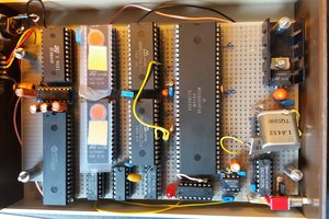
Ian Bradbury's design uses an ATV750 which is like two 22V10 chips in one package, and each output macrocell can have its own clock and set/reset signals.
His logic makes much use of the latter, which is useful because the ZX80 circuit also has multiple clocks and set/reset signals. For that reason I am currently keeping the 74HC74 D-type latches.
The HSYNC logic of the ATV750 will not fit in a 22V10, so I decided to use a 74HC393 counter and a 22V10.
... Read more »2023-08-28
I looked at Ian Bradbury's ZX81 in SPLDs, intending to mop up some of the small-scale-integration chips (2 to 4 input gates) that I don't have, into 22V10 logic chips that I do have. They're handy because they operate at 5V.
The logic is written in CUPL which is quite low level, like assembly language. Most designers have moved on to VHDL or Verilog, which are needed for today's big FPGA chips.
I thought I'd have a go compiling one of the ready-made designs.
There's a Cyclone II EP2C5 Mini Dev Board available dirt cheap and ZX81 code for it at https://www.qsl.net/yt2fsg/zx81/zx81_clone.html which I downloaded, unzipped and opened the project file from Quartus.
First of, it complains that my version of Quartus Lite, 20.1.1, will not compile for Cyclone II.
Okay, I told it to compile for Cyclone IV, which is the device on the DE-NANO that I have.
Next is complained T80s not found. This Z80 model is someone else's project, so I guessed I need to get the latest version.
I went to https://github.com/mist-devel/T80 and downloaded the files as a zip file called T80-master.zip which needed unzipping into a sibling directory called T80. It unzipped into a directory called T80-master so that needed renaming. That fixed that issue.
Now it moans:
Warning (12019): Can't analyze file -- file ../FPGA_ZX8x_shared/*.vhd is missing
where *.vhd is many files. The whole directory is missing!
I eventually found this to be a better source of everything:
https://svn.mavipet.sk/svn/fpga_comps/HW_V1.0/
most of which are Cyclone II but FPGA_ZX81_Full does not get the Cyclone II error message.
But I still get other errors!
2023-08-31
One can add slow mode hardware to a ZX80, but I decided to buy a board with this designed in already.
2023-08-19
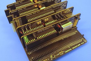
I bought these boards on eBay.
The logic board has some nice features. The bus signals are available on a holes for a header, allowing the dreaded RAM-pack wobble to be avoided. The board can take up to 32K RAM, so you don't even need an external RAM pack.
Power is from a USB-B socket. I'll have to check the electric current budget.
On the down side, the clock is a crystal-and-inverter which mean I can't change frequencies by swapping an oscillator can. I think that can be hacked!
The on-board SLOW-mode generator will need hacking to run with a 14.7456 MHz clock. I'll design something that can be easily switched between two frequencies.
The keyboard is on a separate PCB, so no mechanical stress is transmitted to the motherboard. It has the key letters but not the associated keywords.
The boards are due in about a week, so I shall get hunting for components.
2023-08-21
Printed out the circuit diagram and parts list. I have:
What I don't have:
I could use some PAL chips to mop up the random logic. I have plenty and they are easy to modify.
2023-08-23
Boards arrived. I have soldered the key switches to the keyboard.
The motherboard is very packed.
2023-08-25
I fitted 0603 surface mount resistors where there are vertical through-hole resistors.
The ACT574 and HC165 chip are now soldered to the board.
2023-08-31
I have no HC541 chips but plenty of HC245 chips. So I took two HC245 chips and bent pin 1 under the chip and wired it to VCC. I then fitted it to the HC541 sites.
2023-09-27
Fitted SIL sockets for keyboard.
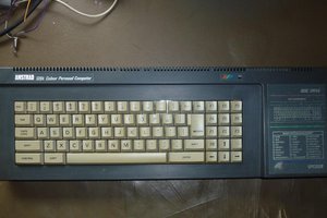
This was the quickest way of getting a known-good reference machine.
Alas it is not very hackable, because most of the logic is inside the ULA.
It did come cased with a working membrane keyboard.
I extended the connections to the keyboard using extra-flex wire, allowing operation with the PCB accessible without removing the membrane from the case.
I hacked the ROM socket to accept a modern flash ROM, so that I could experiment with modified firmware.
I removed the 5V regulator and heatsink then wired a 2.1 mm power socket so that could be powered by a common 5V wall-wart power supply.
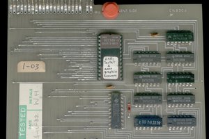
Attached is the G007 graphics board. I have tried to reduce the RAM-pack wobble by fitting a 32K RAM chip over the G007 ROM chip. D7 and D6 have to go to the edge connector. This should be an easy hack but for some reason it didn't work and I left that hack in that state. It still works with an external RAM pack if the 32K RAM is removed.
2023-09-15
Not working right now, I checked the ROM and RAM address lines. I tied the ROM /WE pin high. Seemed not to work but I had set my TV for white-on-black for my ZX80. Adjusting the controls allowed the ZX81 signal to be seen.
Still not working with the G007, or the DRAM pack, or both.
Create an account to leave a comment. Already have an account? Log In.
Become a member to follow this project and never miss any updates


 Hacker404
 Keith
Keith
 Colin Maykish