Goals
- Low cost - TBD should be affordable enough to use as a component in a project
- Easy to program - TBD's functionality should be controllable through a minimum of coding. TBD's dev tools should require a minimum of effort to install and configure
- I/O support - TBD's I/O pins should encompass as many hardware inferfaces as possible. At a minimum TBD should support 1 channel each of SPI, I2C, and UART though not necessarily at once.
- Upgradable - TBD should be programmable by a USB host using simple tools
- Unbrickable - TBD's micro should contain a bootloader in ROM that can be forced to run by hardware strap
- Small - TBD should be as small as possible so that it can be always available in a portable toolkit
Hardware
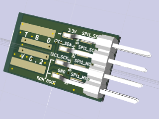
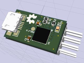
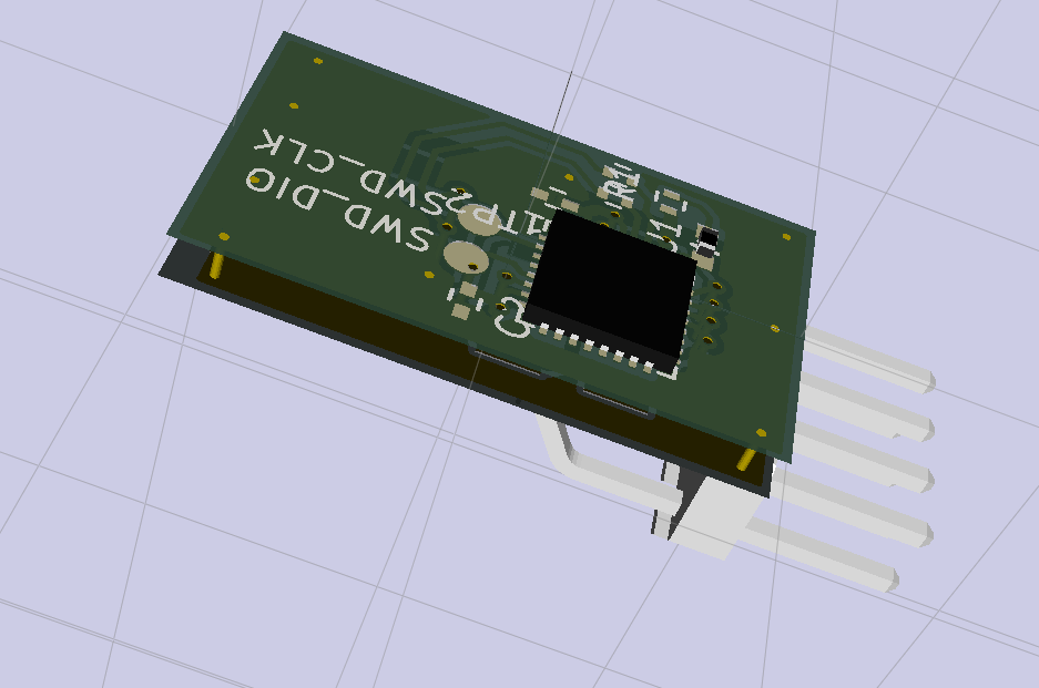
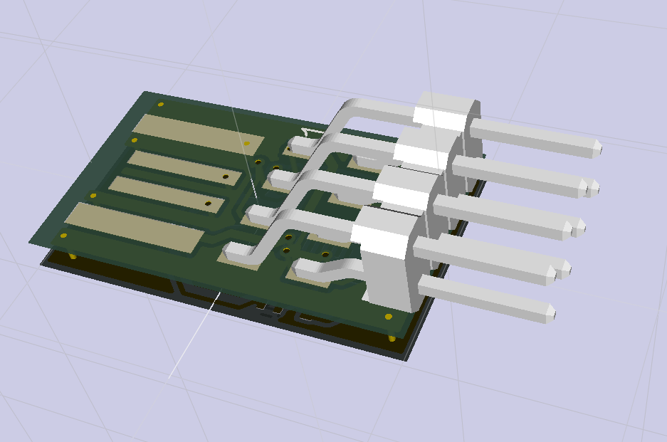
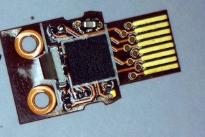
The TBD board connects a USB host to 6 I/O pins by way of a Freescale KL27Z ARM microcontroller. TBD's PCB is sized so that it plugs directly into a USB port, and has pads so that no additional USB connector is needed. A plastic shim on the opposite side of the USB-A pads insulates the PCB from the port frame and improves the fit and contact with the port. I/O is exposed on an 8 pin 0.100" pitch dual row pin header. The header is an SMT right angle style that minimizes the overall length of TBD. Overall height of the PCB and header leaves sufficient clearance for other USB plugs above and below the board when plugged into a stacked USB-A port.
A Freescale Kinetis MKL27Z256VFM4 microcontroller is at the heart of TBD. Few other components are required: bypass caps, USB and LED current limiter resistors, connectors, and the LED are the only other parts on the PCB. The KL27Z micro contains a 48MHz ARM Cortex-M0+, 256K flash, 32K RAM, various peripherals, 5V to 3.3V linear regulator, and a 16K Kinetis Bootloader ("Kibble") ROM. An internal trimmed oscillator provides the core and most of the peripheral clocks, while the USB device interface is "clockless" by way of clock recovery from the USB host, so no external crystal is needed. The on-chip 3.3V LDO steps down the USB bus power to the 3.3V chip supply, and is available on the I/O header to power low current devices.
The I/O header exposes ground and 3.3V as well as 6 pins that are multiplexed for GPIO, I2C, SPI, FlexIO (Freescale generic serial interface), UART, timer, and ADC. One pin (I2C1_SDA) is sampled by the micro on power-on and will force the ROM bootloader to run if pulled low. This pin is situated next to GND so that a 2 pin jumper can be fitted over both. All I/Os on the header are directly connected to the micro without any current limiting, filtering, or other protection. This is common and almost expected for other similar micro dev boards.
(todo: insert pin map / mux table)
An LED connected to one of the GPIOs can be used by software for status.
The PCB is made with all SMD components located on one side except for the header. Stencil / paste / reflow is used to solder the component side, while the header is hand soldered. The LED and passives are all 0603 size, while the micro uses the 5x5x1mm QFN-32 package.
Software
Toolchain : mbed
Coding for TBD is done using the mbed library. The plan is that eventually (somehow?) TBD will be supported in the mbed web-based online IDE, making development possible with nothing more than a browser.
For now the mbed library can build TBD-compatible projects offline using the KL43 target, a package variant of the silicon used in TBD. This takes much more effort to use than the online IDE, and detracts from the convenience factor TBD promises.
The Freescale KDS / KSDK IDE can be used as an alternative, but is also not as simple as the mbed online IDE.
Flashing : kut
kut is a Chrome browser app that uploads new firmware to the KL27 micro in TBD over USB. Uploading new firmware to TBD with kbl is as simple as choosing a file from the local disk, putting a jumper over two pins on TBD (clearly marked in the silkscreen), and plugging TBD into the PC. As a local Chrome app, kut can access certain USB devices and local files without needing device...
Read more » ajlitt


 WestfW
 Sam Ettinger
 Stephen Holdaway
This is a really impressive project... I LOVE the idea, and would certainly buy a couple assuming the price was reasonable. A couple of random / stupid ideas:
1. The thickness of a USB connector just happens to be exactly the distance between the pins of a standard 2 row header: 0.075" So.... Use a thicker PCB stock, 0.062" is close enough with a layer of solder, and use a standard header, but put the PCB between the two rows of pins. So the SMT pads for row 1 are the top of the PCB and the SMT pads for row 2 are the bottom. This takes less board space and you can then avoid the need for the plastic shim because the PCB stock is thick enough to just plug into the USB port on it's own.
2. Careful arrangement of the IO pads on either side of the PCB might allow for transistors to be placed at the edge of the board instead of the header. The amplified signals could then be used to drive small motors, relays, etc… (see 4. below) Ground on one side, signal on the other and the transistor is installed with base to ground, emitter to signal, and the collector run into a terminal block placed flat on the PCB and held on with double back tape. The other side of the terminal block goes to the load, and the other side of the load to unregulated power. Not sure I explained that well enough... I can add a picture.
3. Check out the TI Tiva C Series which also comes with a USB bootloader. As does ST STM32F042/072. The PIC18F46J50... might... not sure.
4. To avoid future USB port loss or maybe even PC loss, consider adding / using a USB isolation system like the Analog Devices ADUM4160
Here is the reference design:
http://www.analog.com/en/design-center/reference-designs/hardware-reference-design/circuits-from-the-lab/cn0160.html#rd-description
Actually, that could be a separate project entirely: A USB port isolator for development projects. It's been done, but not as a USB to USB device:
http://hackaday.com/2014/04/27/galvanic-isolated-ftdi-saves-your-computer/
5. Really whacko idea: Coin Cell Power! A pair of holes in the +Vcc rail over a ground plane for a paper clip coin battery holder would allow independent operation at 3 volts.
http://dangerousprototypes.com/forum/viewtopic.php?f=2&t=5635
So you program it with the USB plugged into the PC, then you unplug it, solder on the paper clip, slip in the coin cell, and it's up and running. I /think/ you could place those holes on the USB connector end, with the ground plane on the back of the USB, so it wouldn't take up any more space. The coin cell would hang out over the edge of the PCB that used to be the USB connector.
Yeah... that was pretty crazy, so I'll stop there. ,o)