 drewrisinger
Overview
For this project, I had a very simple goal: be able to easily program the ESP8266 modules. Since I bought a few different varieties, I wanted this board to be compatible across as many as possible.
Goals
- Program ESP8266
- Access all possible communication lines to ESP8266, preferably on a breadboard
- Provide regulated 3.3V power to ESP8266
- Create a small and cheap board that could be used standalone or integrated into other projects
- Buttons to enter programming mode, or to reset
Schematic
This schematic was created using NI MultiSim. It was modeled on Adafruit's Huzzah ESP8266 board, though with several changes, such as:
- Switch to change between regulated and unregulated power
- Omitted several parts of Adafruit's board that I considered unnecessary (diode protection, etc)
Schematic Summary
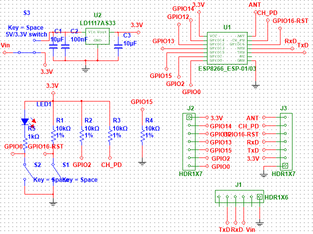
The schematic should be read nonlinearly. Signals come in through J1 at the bottom right (Vin, TxD, and RxD). Vin then runs through a switch to select between 5V (or greater) and 3.3V (pre-regulated) input power. Essentially, this switch (S3) acts as a voltage regulator bypass. U2 is the 3.3V regulator, which is stored in C3.
Next, the bottom left section sets several lines to their default values, using pull-up and pull-down resistors.
- GPIO16 (Reset) is pulled high except when the reset switch (S1) is closed, which sets it to ground and will reset the ESP8266.
- GPIO0 is pulled to ground when S2 is closed to enter programming mode. This needs to be pushed on reset. Note: LED1 will light when S2 is pushed to provide feedback.
- GPIO2 is pulled high.
- CH_PD (Chip power down) is pulled high to keep the chip on under normal situations. This can be pulled low to put the chip in its power down state.
- GPIO15 is pulled low.
BOM
Version 1.0 of the BOM (corresponding to v1.0-1.5) can be found at GitHub
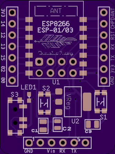
Layout
Version 1.5 OSHPark Renders
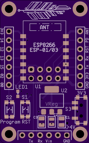
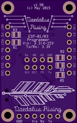
The layout was made using NI Ultiboard. This is version 1.5. The board size is 1.60"L by 1.0"W.
Building
Here you have your choice of ESP-01 or ESP-03 module. If you have an ESP-03 module to mate with this board, you can simply solder its castellated pads onto the provided solder pads in the provided U1 section. If you have an ESP-01, you solder a 2x4 female header onto the provided pins in the center of the board, and then plug the ESP-01 into it in the orientation denoted on the board.
This is probably a challenging soldering build due to the small feature size of the components. There are many 0805 (8 mil by 5 mil) and 0603 (6 mil by 3 mil) components, which take a steady hand to solder, but should still be doable.
I highly recommend doing the SMD components first, and then adding the thru-hole headers on later.
I will update this section once I have the board and components, and can actually put the board together.
Future Improvements
In future versions, there are several things that I would like to do to continue this project:
- Minor improvements to layout, such as labeling and clarity. (completed in v1.5)
- Add Breakouts for other ESP modules
- Create breakout variant with micro USB connector and USB-> Serial chip such as CH340G so a separate serial chip isn't needed. Unfortunately, this will add size to the board, as well as making the board more difficult to solder.


 anfroholic
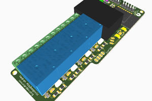
 nardev
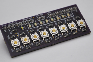
 Charlie
 Torbjörn Lindholm
Nice!!!!
Ordered 10 boards using your gerbers from JLCPCB for $5....can't wait to get em in
Great job and great design!