Yann Guidon / YGDES
-
Barrel Shifter (3)
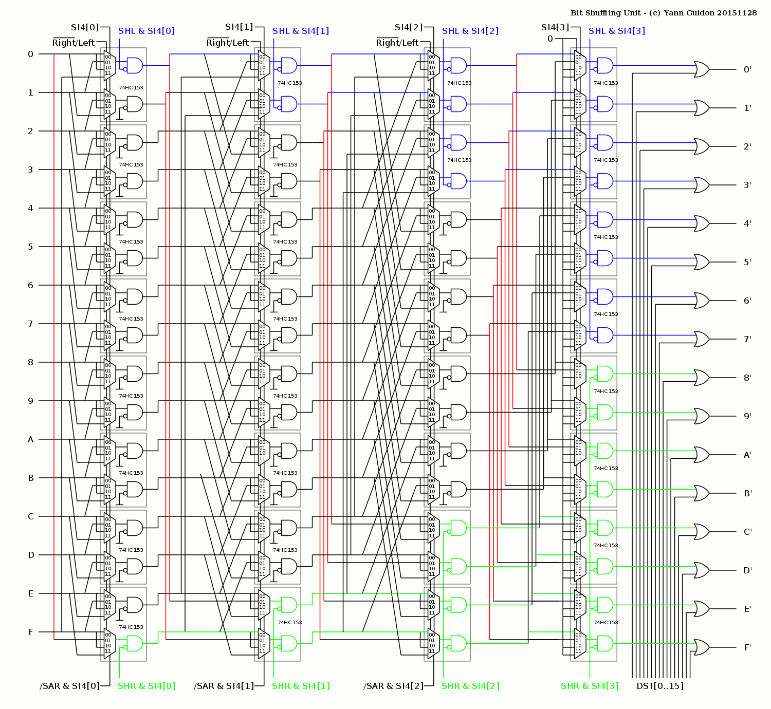
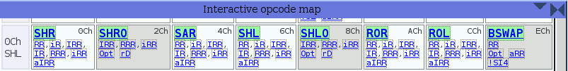
11/28/2015 at 20:22 • 6 commentsAfter more work, here is the circuit diagram for the SHL unit!
![]()
I have tried to make the function a bit more apparent by using some colors.
One cool detail is that the last stage is just a "swap" layer, made of MUX2. However, it is more interesting to keep the '153 because it contains 2 AND gates so if a '157 was used, a half 74HC08 would be needed.Here, some inputs are wasted but the circuit's structure remains very regular. The unused inputs might also be used to extend the functionality of the unit, with finer insert/extract operations.
The chip count is 32×74HC153 (dual MUX4 with enable), 4×74HC32 OR gates and some more logic for the control. Some more '08 might be needed to mask some bytes of the DST operand.
The critical datapath is 5 circuits, which is pretty good for such a versatile circuit. Indeed, it can also perform the operations of the IE (Insert/Extract) unit that manages/aligns bytes from/to memory (more control logic is required though).
Many AND inputs are tied to 0V. This could instead be tied to a global "enable" signal that reduces signal swings in the unit and save some power.
I think that this unit is very cool, despite its significant size. Though it would be worse with transistors ;-)
-
The 74HC138/154/238 as a (almost) universal logic gate
11/26/2015 at 10:53 • 0 commentsThe 74HC138 is a pretty awesome circuit. It can be used as a 6-inputs NAND gate with up to 4 inverted inputs. It even has 8 outputs !
If you prefer the AND function, use a 238 instead. And the '154 has 16 outputs!
For a more universal/arbitrary logic function, add some OR gates to the outputs: this provides XOR and MUX behaviour. And if you can do a MUX you can do a latch!
At this moment, I'm struggling to find decent prices for "littlegate"/"single gate" ICs (in the 74LVC1G and 74LVC2G family). The 74HC138 can be found in decent quantities at decent prices and will probably replace a few gates, for example for decoding logic (I'm looking at the UP/DOWN strobes of the register sets at this moment).
-
Instruction sequencing
11/26/2015 at 10:32 • 0 commentsThis log is both an introduction and a "note for later" about the scheduling of the control signals.
The Discrete YASEP is derived from the microYASEP but due to technology differences, the scheduling can't be reused as is. The microYASEP uses DFF latches, which make it a fully synchronous design (alternating layers of DFF and logic that can be pipelined). However the Discrete YASEP uses 74HC193 up-down counters for the registers, their behaviour for the preload timing makes them look like transparent latches.
Because of this (and other architectural factors), the operands are latched in the input of the ALU. This prevents data from looping or become unstable in the case where a register is both a destination and source for a computation.
This makes the design a 2-cycles system:
- the first cycle fetches the operands from the registers (or memory) to be latched in the ALU
- the second cycle computes the operation then latches the result(s) (if the condition is evaluated as true) in the destination register (and might update others as well).
Each cycle has sub-cycles as well. The sequencer needs a higher clock input frequency, at least a four-phases clock where the phase 1 latches the operands and phase 3 latches the results, but it's more complex than that because both cycles have a different latency and the scheduling changes a bit between short and long instructions (due to the long immediate operand).
(to be continued)
-
Memory editor
11/25/2015 at 22:03 • 0 commentsThere is a feature that I want to include in the system : a hardware assembler/disassembler, which could also be called "instruction editor". Today, I realised that it's a very desirable feature but it was too shortsighted. Editing a value with TTL chips is cool but this must be well integrated/interfaced with the rest of the system.
The first issue is how to access memory banks. Normally, it's done through the A/D registers but during debug, this is less... practical. Even less when the A/D pair triggered a breakpoint, then we have to save the value for later restoration after we have modified them to explore the memory bank.
So the read/write feature is not just required for the instruction memory but also data memories. The editor must be generalised and should also edit arbitrary numbers, not just instructions. Instructions already contain data fields so the instruction editor can be considered as an extension of a more basic memory editor...
Another question is how to save/restore the A registers while they are being temporarily altered. I have come to the "less hacky" solution where the address registers are not modified. Instead, their counter's outputs are multiplexed with another value (probably coming from the PC bus but it could be another special "debug" bus) that is controlled by the memory editor. The user then selects which memory array is selected.
Of course, multiplexing the address takes many precisous nanoseconds but convenience trumps speed in our case.
-
Flash EEPROM adventures (and a happy end)
11/25/2015 at 04:31 • 8 commentsAfter I got an old EEPROM writer working, I started creating a multiply table with old BIOS PLCC32 chips.
However this is good only for the DIP prototype working with 5V. The 3.3V system needs to use SMD parts only.
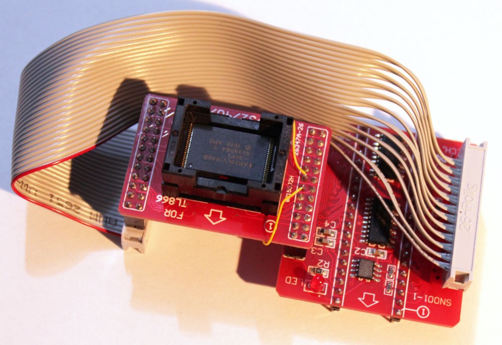
I spent more money on modern gear and found a good deal on eBay for a TL866A universal programmer. It arrived lately ! You can guess the excitment... I'm still not sleeping ;-)
So I tried all the old BIOS chips I had around and all pass (except some weird under-marked chips from an undefined manufacturer but who cares).
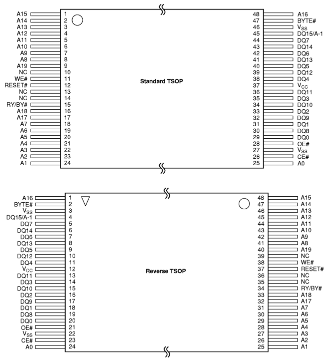
Next comes the time to try the Am29LV160DB and use the fancy TSOP48 ZIF adapter. No luck. I try everything : no result. Some garbage appear but... it doesn't work.
Is the active adapter broken ? That could explain it but it's brand new...
I've turned the problem around and around in my head and no solution. Time to read the datasheet again. And...
Wait, what ?![]()
They sell the very same chip with the pinout totally reversed ?
Now that might explain why I see this unusual triangle on the topleft corner that did not ring a bell (until now).
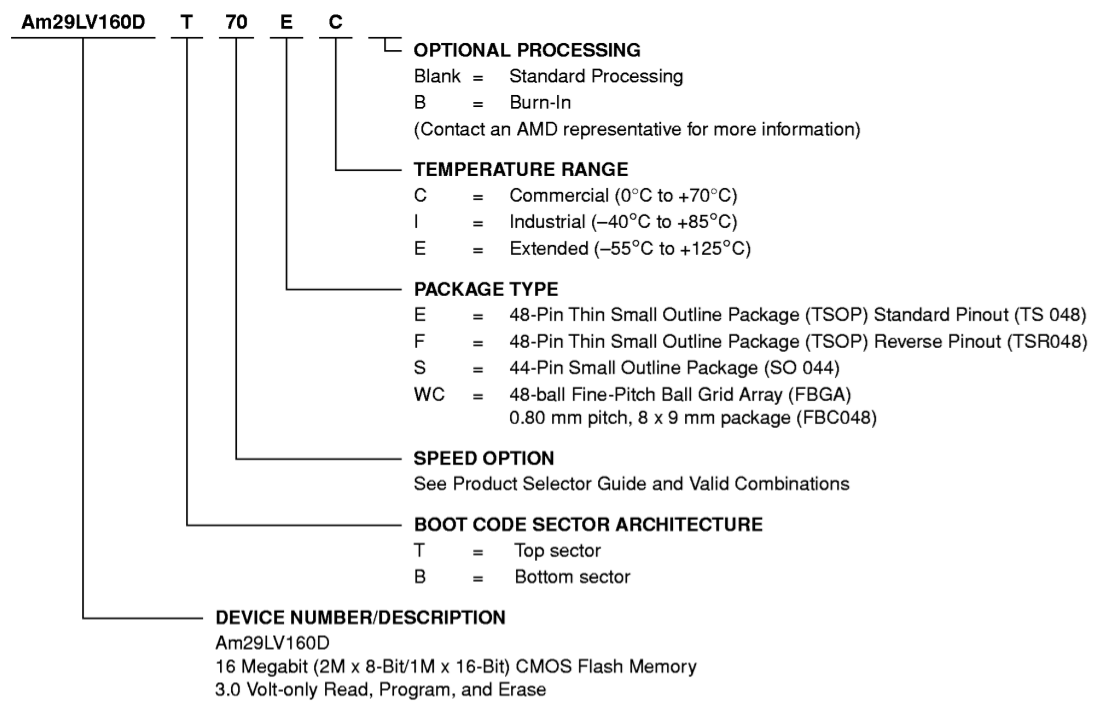
The part is more precisely : AM29LV160DB-90FC and the software only cares about AM29LV160DB. What do the next signs mean ?
"F" means reversed pinout... I might have burned 3 chips to get this detail !Now, how do I reverse the pins ? Inserting the chip in reverse in the ZIF socket does not lock the pins. I apparently have to make an adapter board... (there are already 2 PCB for adaptation and it's getting ridiculous now).![]()
The other solution is to solder another female connector on the other side of the ZIF's PCB :-D Soldering will be "interesting" because there are 2 rows...
Update
The new adapter adapter works !
It was not as easy as I thought because the naive version also reverses some pins (differently). And I broke two pads while removing the aforementioned female connectors from the ZIF board (hence the yellow patch wires). But with some twisted IDC magic, all the "guinea pig" chips have been programmed, none was even fried from the precedent attempts with the wrong connections.
![]()
I wasn't sure what to expect from the TL866A but so far, it seems to work well. I hate having to use Windows but I think the programmer will be useful in the future :-)
-
Barrel Shifter (2)
11/24/2015 at 10:58 • 0 commentsThe precedent log had a few flaws that I will correct here ;-)
The main flaw was to try to design the logic "in my head" so here is the detailed "equation" for one level of shift, considering an hypothetical 4-bits input, with bits named A, B, C and D (it would still work with only A, B and C but I'm feeling generous).
Inputs D C B A SHL 1 C B A 0 ROL 1 C B A D SHR 1 0 D C B SAR 1 D D C B ROR 1 A D C B From there, the circuit is straight-forward to draw:
![]()
Repeat and expand: 16 bits instead of 4 in length, and 4 layers instead of just one.
The adjustment logic on both sides will grow in depth, from 1 bit in layer 0, to 2 bits in layer 1, 4 bits in layer 2 and 8 bits (one half on each side) for the last layer. This is where we see the advantage of the integrated AND gate included in each '153 as it adds no overhead :-)
Some overhead is in the decoding and control logic, that is not completely represented here. The /Right/Left signal would ideally be directly coming from the instruction word, if it was better organised, so here is a new attempt:
- Left/right are one half each of the instruction group.
- There are 3 left operations and 4 right operations so the BSWAP operation is tucked in the left operations
- There are 2 shift operations per direction (with and without OR), plus one rotation. The remaining is either arithmetic shift (SAR) or BSWAP which should have the same position in their respective group (let's say the 3rd so they are easy to decode).
The instruction bits are allocated in the SHL group:
- bit 2: direction (0: right, 1: left)
- bit 1: Shift/rotate (0: shift, 1: rotate or special op)
- bit 0: OR or special op when 1
The opcode can easily be decoded with a simple 74HC138 or '238, depending on the needed signal polarity, and (N)AND gates do the rest in the circuit.
The codes are thus derived:
- 0 : SHR
- 1 : SHRO
- 2 : ROR
- 3 : SAR
- 4 : SHL
- 5 : SHLO
- 6 : ROL
- 7 : BSWAP
In the case of BSWAP, the SI4 operand MUST be 0 and the decoding logic will do the swap at the last layer.
I think I like this design :-)
-
Barrel Shifter
11/22/2015 at 17:48 • 0 commentsOne of the units of the YASEP is called SHL, for "SHuffLe" unit. It performs bit shift and rotations:
![]()
- SHR is SHift logic Right
- SHRO is SHR then OR with the destination
- SAR is Shift Arithmetic Right (preserves the MSB)
- SHL is SHift Left
- SHLO is SHL then OR with destination
- ROR is ROtate Right
- ROL is ROtate Left
- BSWAP amounts to a rotation by 8 bits for YASEP16, byte swap for YASEP32.
All these operations are grouped because they use a barrel shifter (plus a OR layer of SHR0 and SHLO). The purpose of this unit is simply to move bits around (to shuffle them).
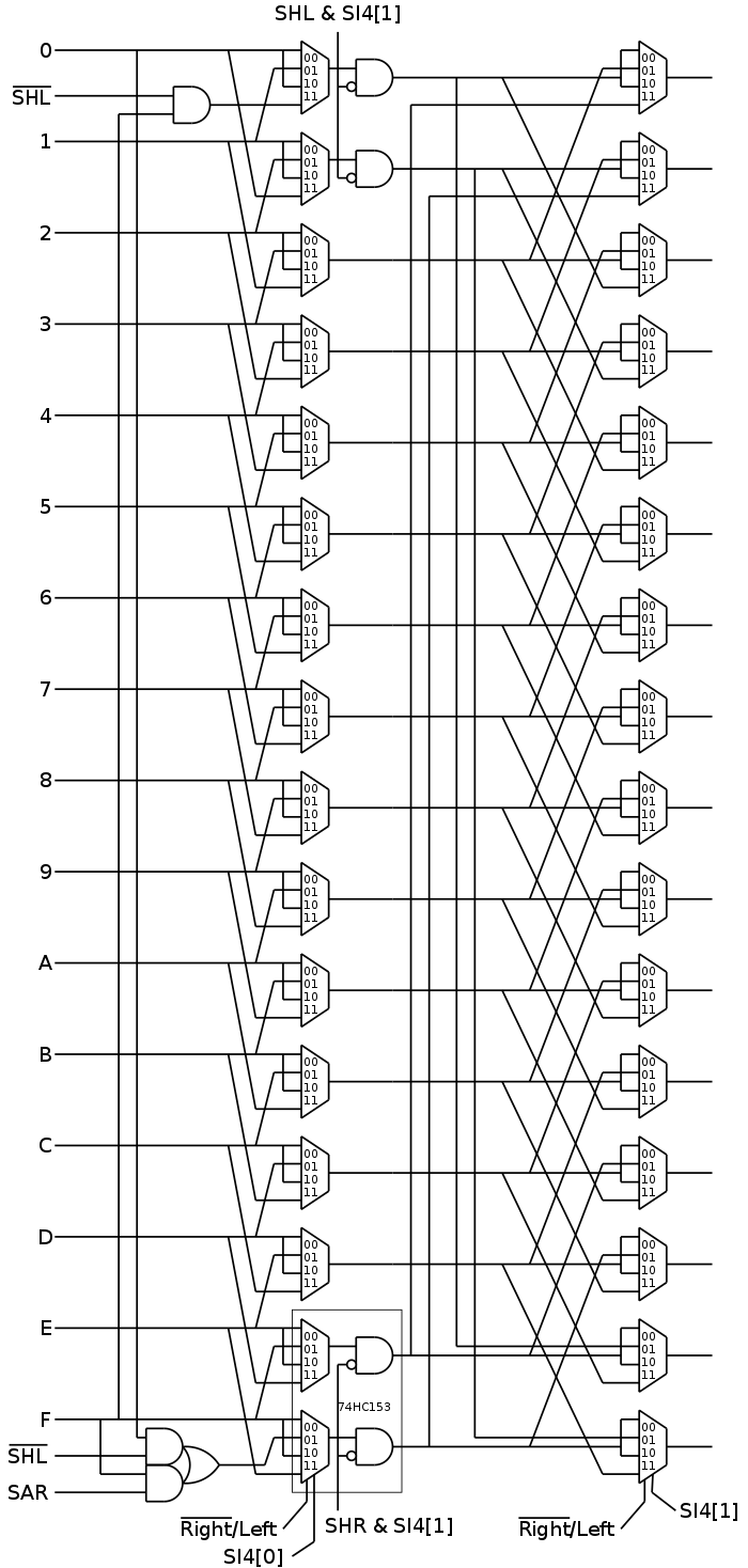
The structure of the barrel shifter is centered around several layers of multiplexers:
- Bit 0 of the shift amount operand will shift the data operand by 0 or 1 bit
- Bit 1 shifts by 0 or 2 bits
- Bit 2 shifts by 0 or 4 bits
- Bit 3 shifts by 0 or 8 bits
The last layer is used for BSWAP, with all precedent layers not shifting.
Mixing shift and rotation makes it a marginally more complex, but mixing left and right shifts, with arithmetic/logic options becomes pretty complex with MUX2s (74HC157).
However with the 74HC153, things become pretty simple again: it's a dual MUX4 so each bit can select between "pass", "left", "right", "another right" (for sign extension) and even 0 because each output can be cleared. With 4 layers of 16 bits, this amounts to 32×74HC153 (only). If we add the last OR layer, this is 36 chips, without the control/decoding gates (and buffers).
![]()
The '153 is also a bit easier to route, as well, as seen when studying the register set.
The preliminary diagram looks like this:
![]()
(I know it's not working well but it's a start)
-
Input FIFO (continued)
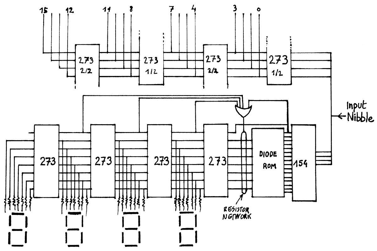
11/13/2015 at 18:14 • 0 commentsWith the diode ROM that "solves" the hexadecimal-to-7segments problem, it's now time to revise the design of the input FIFO.
The 4-deep and 4-wide "shift register" is implemented by the same 74HC273 as before, this does not change (heh, it works, right ?). So 2× '273 are used for this function.
The changes are in the display logic. The TIL311 are nice for prototyping but they are expensive, not mass-produced anymore, consume a significant amount of power and are not thin or surface-mount devices. The display and decoding problems have been addressed separately, with ultra-thin 4014 LEDs and the diode ROM and it's time to put them all together.
Unfortunately, the diode ROM and the 4014 display are not practical for my prototyping method. I might assemble them separately and cut/saw the PCBs to make modules... I'll have to etch a proper PCB with the right patterns soon.
The input FIFO's display structure has changed because the TIL311 have individual hexadecimal decoders but the diode array can't be reasonably duplicated. The 4 hex digits will share one diode decoder, and a parallel shift register will propagate the value on the 7 segments, just like the nibble is propagated from LSB to MSB.
The '273 has 8 bits and one remains unused for the 7 segments. This extra bit indicates if the digit is '0' (when it's cleared, because it's the direct output of Y0 of the 74HC154) and this is propagated to some more logic to disable leading 0s. By chance, the '273 resets to all-0s so there is no logic inversion to do there.
Another nice trick: it's possible to play with the pull-up resistors of the diode array. Implicitly, it creates a "AND" gate when instead of pulling up, a logic gate decides to pull-down. All the segments will be off, this controls the leading zero digits. This goes a bit further than the schematic in "Redneck" disintegrated 7 segments decoder, where the extra input of the 273 was unused, but we could see the /Y0 output connected to the /CLR pin.
![]()
I have made a first hex display module with the utra-thin LEDs and the only thing I'm not sure, is the series resistor value. I'll see if/how I can make a module that contains all the circuits shown in the above diagram.
Update:
I modified the "leading 0" logic :
![]()
- the first '273's MSB is fed from the /Y0 directly, not from the OR, so when you input 0 after 3000h, the display will become blank
- the OR does not use the value of the last '273 because it will be discarded/pushed away by the next digit anyway.
Now, if a 0 is shifted in after 3000h was entered, the 3 remaining 000 MSB/digits should be cleared. That's some more logic to add to the CLR pin of the '273s... The output of the OR can be sent directly to the 4 CLR pins but this must also be combined with the "clear" external command. The external CLR can be combined by the OR and fed to the 3 MSB digits.
Why 3 digits ? When the input is blank, I'd like to have it display at least a 0 at the LSB so the reset local will not affect the LSB.
Damn I have to update the diagram again...
-
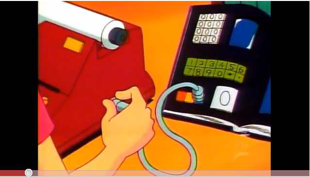
An old question...
11/13/2015 at 00:16 • 2 commentsDid you watch the "Inspector Gadget" series as a kid ?
I was already a big nerd when this aired. When his niece ("Penny", or "Sophie" in french) used that "magic" computer-book, I was looking more carefully... for a few seconds (until that scenaristic clutch became useless for the plot).
![Sophie's computer book]()
And it seems I was not the only one. A simple google search finds many occurences of this. It's an necessary accessory for cosplay and even Boulet had this fascination.
![]()
When I talk to non-geeks and I want to explain them what this project is about, they immediately "get it" when I mention this 30 years old factoid, which has inspired many other people.
And now when I look at this screenshot, I can't keep myself from thinking about how a host computer could communicate with the YASEP system that I'm currently designing...
![]()
No I'm not nostalgic, I just recognize my influences and how and why I became a true geek ;-)
We live in a wonderful era when our kid dreams slowly become true...
-
The registers
11/12/2015 at 10:47 • 0 commentsThis log continues "Registers"
The simplest board of the this project is P3A which contains 4 registers.
There are
- 1 input data bus (the DST/result bus)
- 4 16-bits data latches
- 2 read outputs (SI4 and SND)
The initial plan was very simple: use a bunch of 74HC574. Fanout, fanin and routing created a bunch of problems though.
This approach was abandoned because I decided to move one distinctive functionality into the register set: the discrete YASEP can (and will) perform the register post-update directly at the register level (instead of going through the execution pipeline once again). This simplifies the sequencing of instructions execution: the #microYasep doesn't do post-update, the miniyasep adds cycles (so it's a variable-length pipeline) but here, there is (almost) no time overhead and instructions are executed in two clock cycles, just like the microyasep (but better !).
As a consequence, these are not "registers" anymore but counters. The '574 are replaced by 74HC193, which are preloadable up/down 4-bits cascadable counters. Instead of 4×74HC574 (2 pairs containing duplicated data), there are 4 74HC193 and the load on the result bus is cut in half (this can be further reduced by adding a buffer on the bus but it adds some latency).
Note: not all "counters" are identical:
- for R1-R5, post-increments are +1/-1 (we're talking about them, now)
- For PC, it's the same mechanism but the increment is fixed to +2, the address bits are shifted by one position. The counter is advanced every half-cycle (when it's a long instruction), no post-update is possible. Writing '1' to the LSB, or executing past FFFEh (thus setting the hidden high bit of the PC) will trigger a fault.
- For D1-D5, these "registers" directly map to the memory ports so no post-update possible. The corresponding Areg is post-updated instead.
- For A1-A5, the increments depend on the size of the addressed data. It's normally +2/-2 when D1-D5 is referenced, +1/-1 when A1-A5 are directly referenced, or when IB/EZB/ESB are used on Aregs. Managing the LSB will be tricky, I'm not sure yet how I'll do it. But overflows will also trigger a fault.
Yes, this architecture is not really orthogonal, but the instruction set is simplified a lot!
The advantage of lighter bus load is reduced by the more complex control signals. The '193 is a synchronous counter (with asynchronous reset) but the external data is loaded asynchronously (like a 573, unlike the preferred 574). Fortunately, preload (writeback to the register/counter) seems to have precedence over counting and no special logic is required to avoid conflict, if the control signals are correctly sequenced. However, counting up or down introduces "some delay" as the carry/borrow signals propagate from the LSB to the MSB. Thus, unlike "normal registers", the update of the counters is relatively slow, to overshadow the internal ripple propagation (preload seems to inhibit counting).
This also completely changes the way the conditions are handled. In FPGA/single chip implementations, the conditions are "shadowed"/cached from the result bus. Each register change is captured on its way to the register set and a copy of the condition is kept at a convenient location: the LSB, the MSB and the zero flag.
In this implementation, though, the flags are extracted from the SND bus during the 2nd read cycle. The zero condition can be recomputed, which is great when the condition comes from a D register (data coming from memory, which can't be cached because it doesn't go through the result bus).
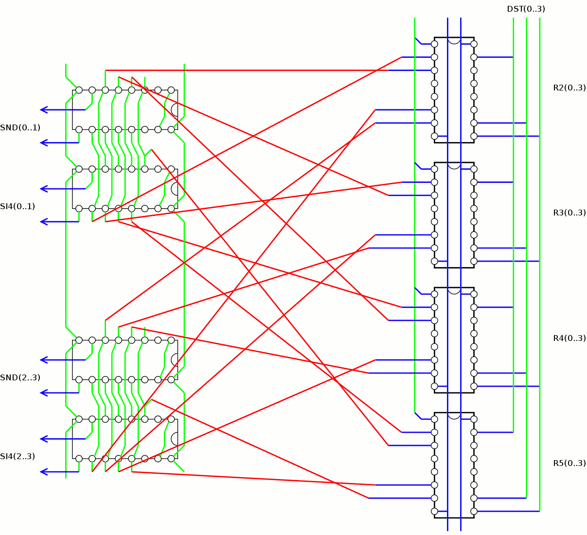
The other problem is the two read buses. It is solved by the many 74HC253 chips: a dual MUX4 with tristate output (so the outputs can also be multiplexed on the read bus from the 3 other boards). As noted in a previous log, this reduces the load on the read buses, which could run a it faster.
Mechanically, there are as many '193 as '253. Each '253 multiplexes 2 bits from 8 inputs so 2×'253 are required to multiplex a bit. But there are two read buses so the number of '253 is doubled. The P3B board contains 16×'193 and 16×253.
Routing is still delicate but there is a hierarchical solution that is suggested by the counters: work with nibbles. One block of 4×'193 and 4×253 can be routed then replicated, the overall net structure looks like a two-levels 16×16 crossbar.
![]()
Note: this layout sketch is not to scale because the '253 are SOIC (1.27mm pitch) and the '193 are SSOP (.635mm pitch). That's why I run wires between the '253's legs on the left and nothing of that kind on the counters (on the right).
Green lines are vertical (on one side of the PCB) and blue are horizontal (on the other side). To keep routing simple, the 253 are on the opposite side of the circuit though I have not mirrored the pinout yet (DIA does not allow miroring or rotations...)
Overall, it looks easily routable :-) Duplicate this 4 times and then connect all the missing lines...
Discrete YASEP
a 16-bits YASEP computer (mostly) made of DIP/SOIC chips like in the 70s and 80s... with 2010's twists!