 Erik Piehl
Link to EP994A files at Github
Fastest TI in the world?
I believe I now have the world's fastest TI-99/4A compatible computer, running at 7 times the speed of the original while using a CPU from 1982, the time when the original TI-99/4A was available.
Old and new happily together
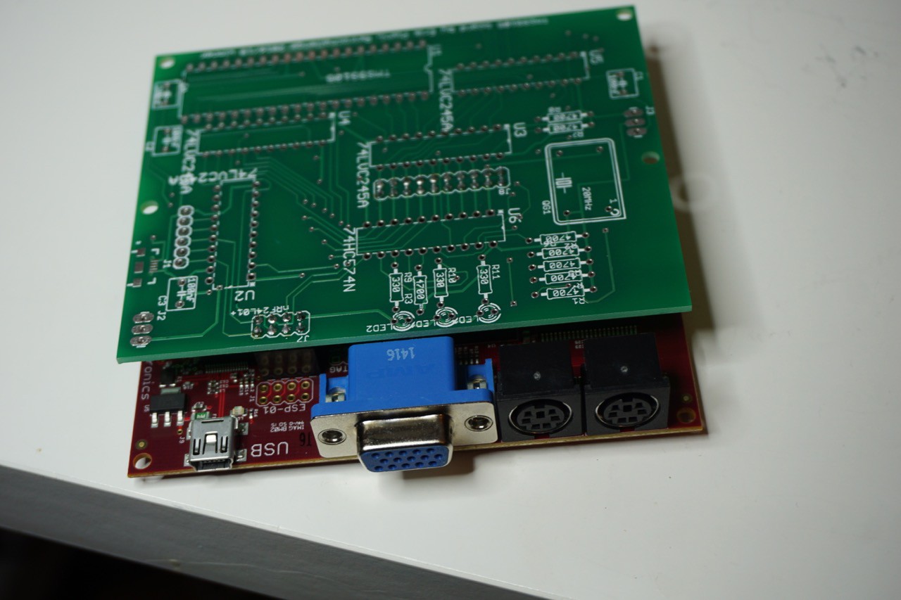
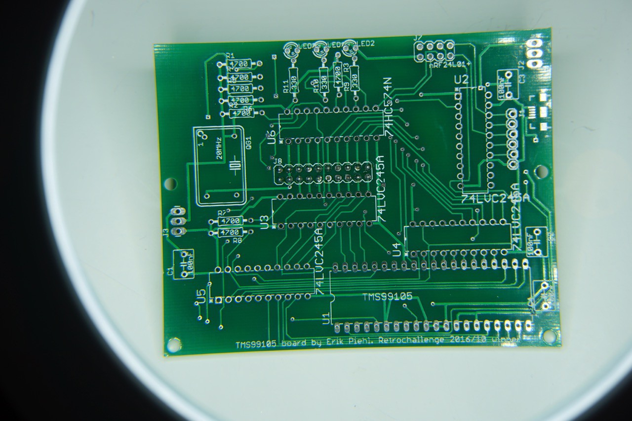
I wanted to combine old and new components, to have that retro aspect. For the "old" part I used the TMS99105 CPU from 1982. This was the fastest processor of the TMS99 range from TI, so a good basis for an enhanced TI-99/4A. For the "new" part I went with a Xilinx Spartan 6 series field programmable logic array (FPGA), to build the rest of the computer apart from the CPU. I wired the "new" and "old" parts together.
Best part of the project: TI 99er community
When I started the project I was looking forward to completing some pieces of a TI-99/4A compatible system. I did not expect to finish the project with something as complete I have now. I did expect to get some feelings of accomplishment as I was confident I could get some parts of the design working. While it was great to have the sense of accomplishment many times over the course of the project (getting the CPU to run, video hardware drawing a screen, Basic booting, games running) that was completely overshadowed by the support I got from the community. So a big thank you to everyone for your comments, advice and encouragement.
The result at the end of October
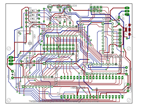
The project logs below describe the various steps I took to build the project, but as a summary these are the components I developed over the course of the project:
- TMS99105 "testbed" on a protoboard, basically I plugged in the CPU chip and a couple of components like the clock oscillator to the protoboard to see if the CPU worked. And it did work!
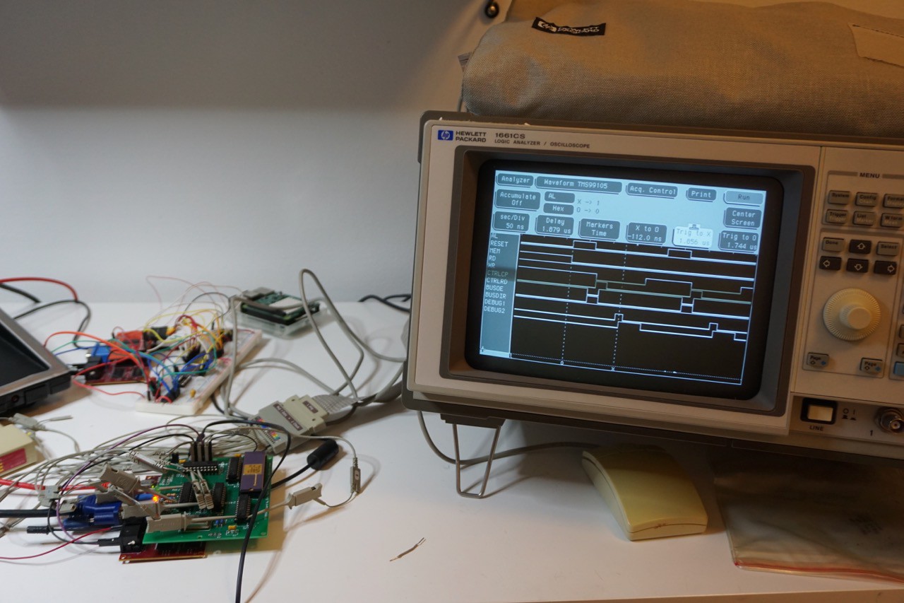
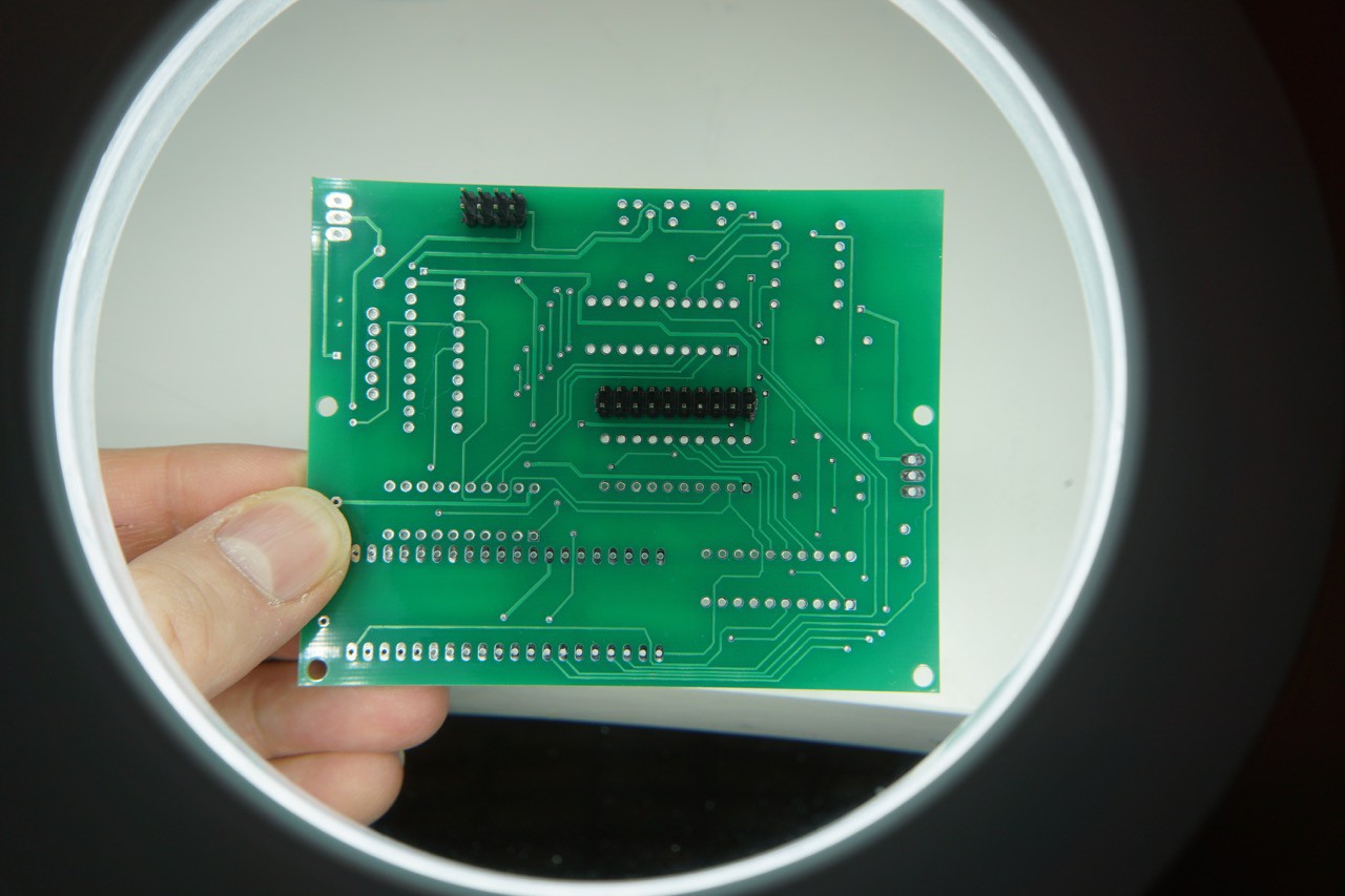
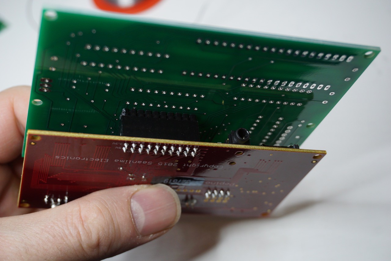
- Wiring up the FPGA: the next order of business was to connect the CPU protoboard to a FPGA board. I used the Saanlima Electronics Pepino development board for thais purpose. So a bunch of wires went between the protoboard and the FPGA board.
- Memory interface: I built a memory interface in the FPGA chip, allowing the TMS99105 to communicate with the memory on the FPGA board.
- Memory loader: I took an existing design of mine, which combines a VHDL component running on the FPGA and a PC host program communicating with the FPGA, allowing me to load software from PC to the memory of the TMS99105.
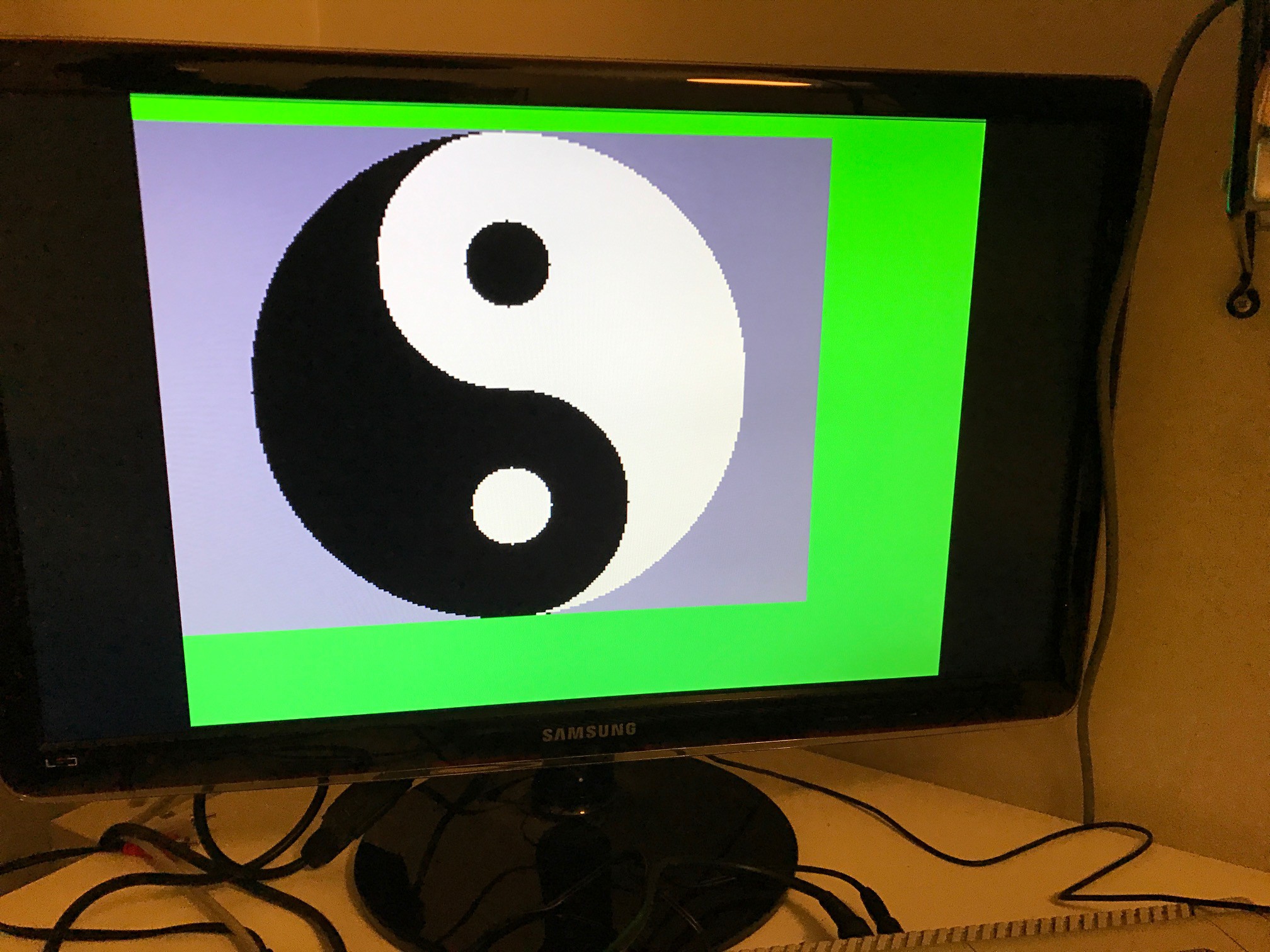
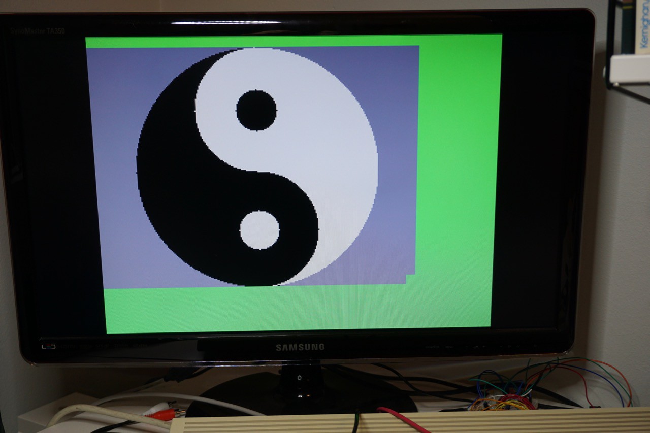
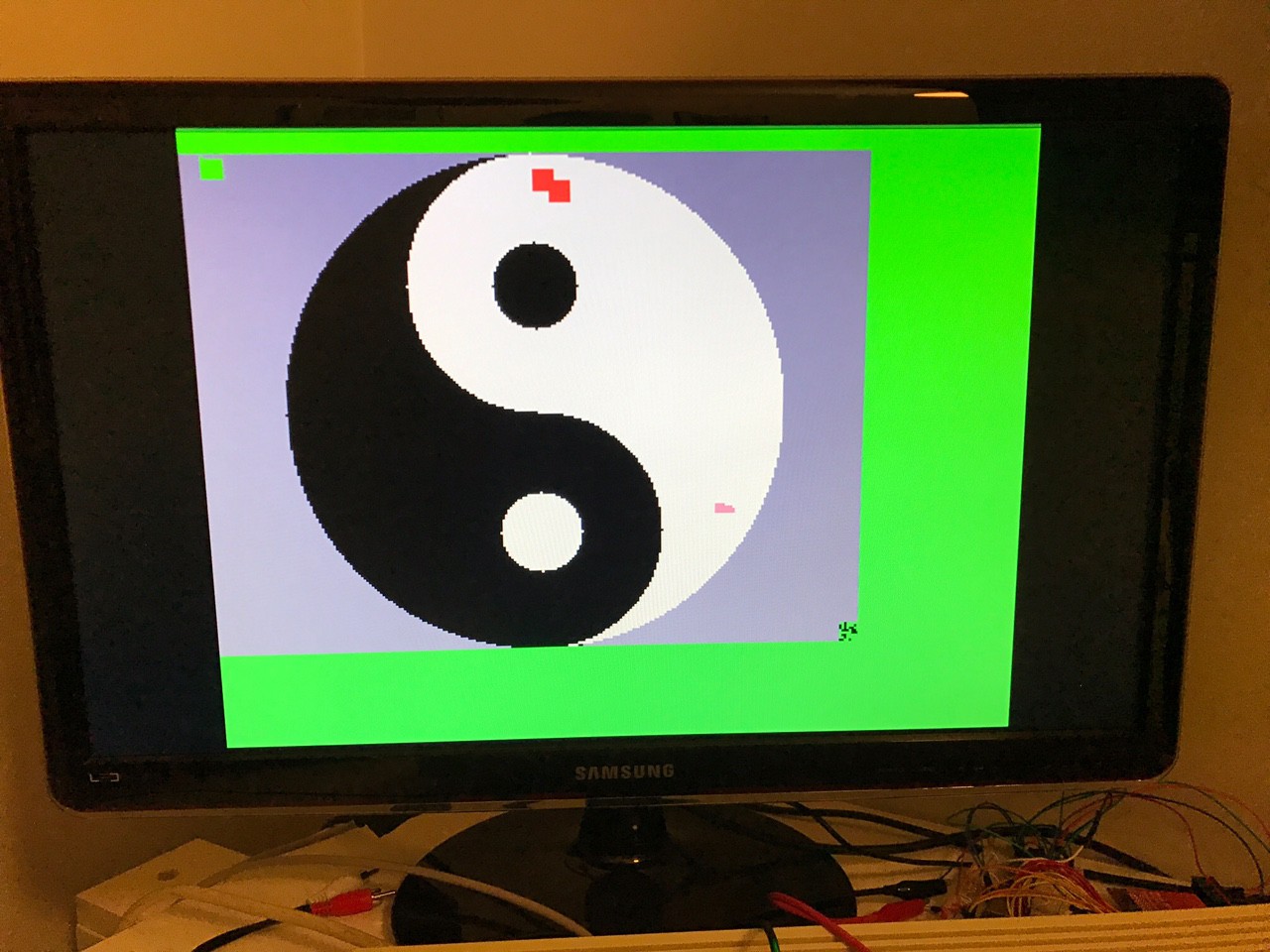
- TMS9918 video processor implementation on the FPGA. This is not 100% complete, but it has support for graphic modes 1 and 2, sprites and scan doubling to allow displaying the video output on a VGA screen.
- TMS9919 sound chip in VHDL. This took less time than I expected and is not completely tested, but I have 3 sound channels and a noise channel so the core features of the chip are there.
- Keyboard emulation: the FPGA implements a portion of the functionality of the TMS9901 I/O chip which is used (among other things) on the original TI to communicate with the keyboard. In my case I use a PC keyboard and a serial channel to communicate the button presses to the FPGA, which presents the keyboard codes via the TMS9901 functionality to software in manner compatible with the original TI.
- Support for banked ROM and GROM, to allow running of TI Basic, TI extended Basic, most games and other software.
Starting point - the beginning of October
This is what I initially wrote about my retro challenge project, in the beginning of October:
Back in the day TI used the TMS9900 CPU for the TI-99/4A home computer. That CPU choice was made due to schedule pressure and led to some strange design choices. TI followed up the TMS9900 family with two other generations of TMS99 family CPUs before the family became extinct: the TMS9995 and the (most powerful) TMS99000 series. My understanding is that no-one has yet tried to build a clone with the TMS99000 series CPU, so I will try to do that with a TMS99105 chip in October 2016 as my retro challenge entry.
Building something like this in a month with very limited spare time is going to be a challenge, to...
Read more »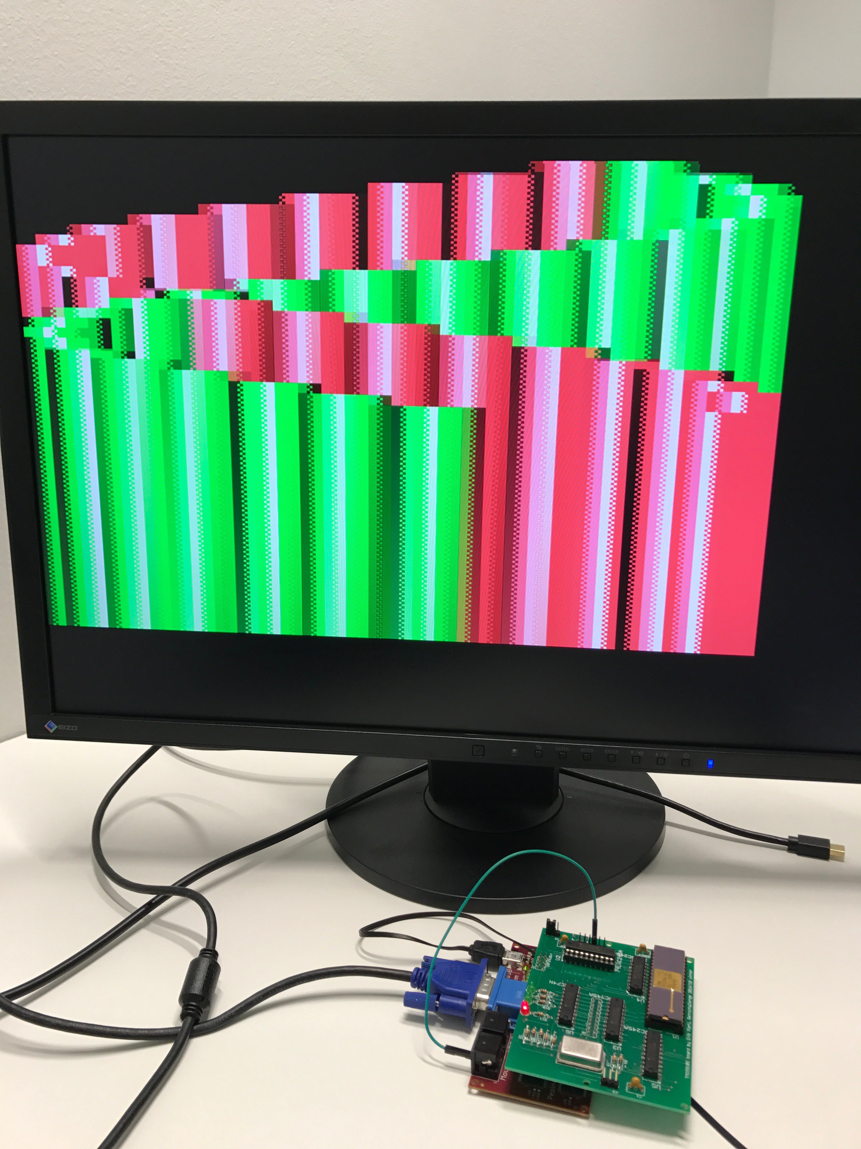


 Leon
Leon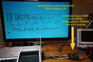
 Matt Stock
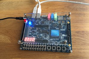
 ErwinM
Hi, I just found this project and it sounds amazing. (These are the sort of things I wonder about myself -- what could have been?) Are there any recent updates on this project?