Ted Yapo
-
A Sharper Edge
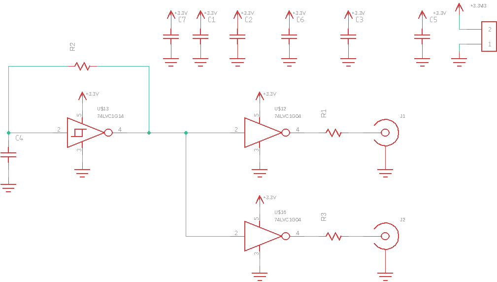
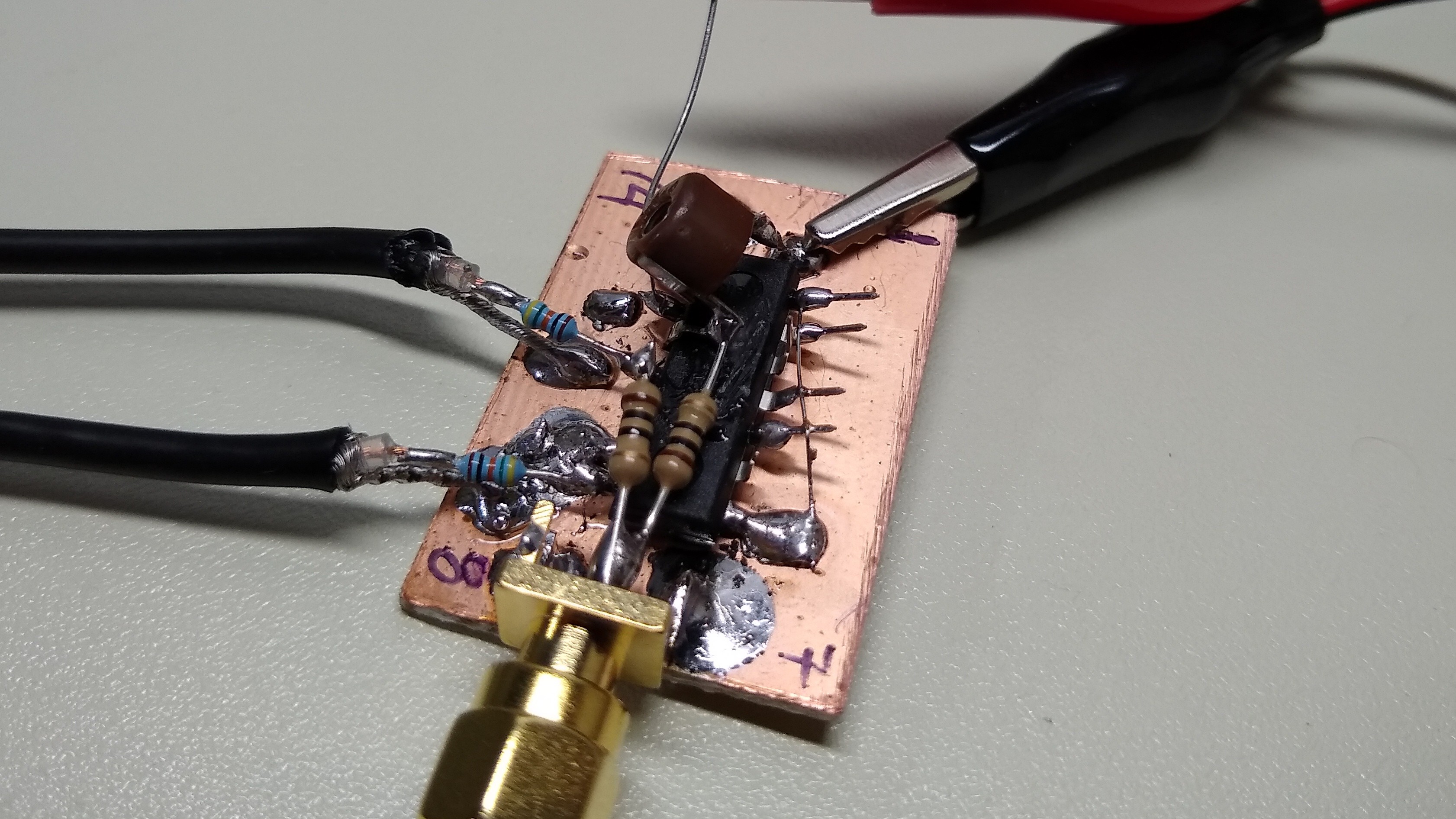
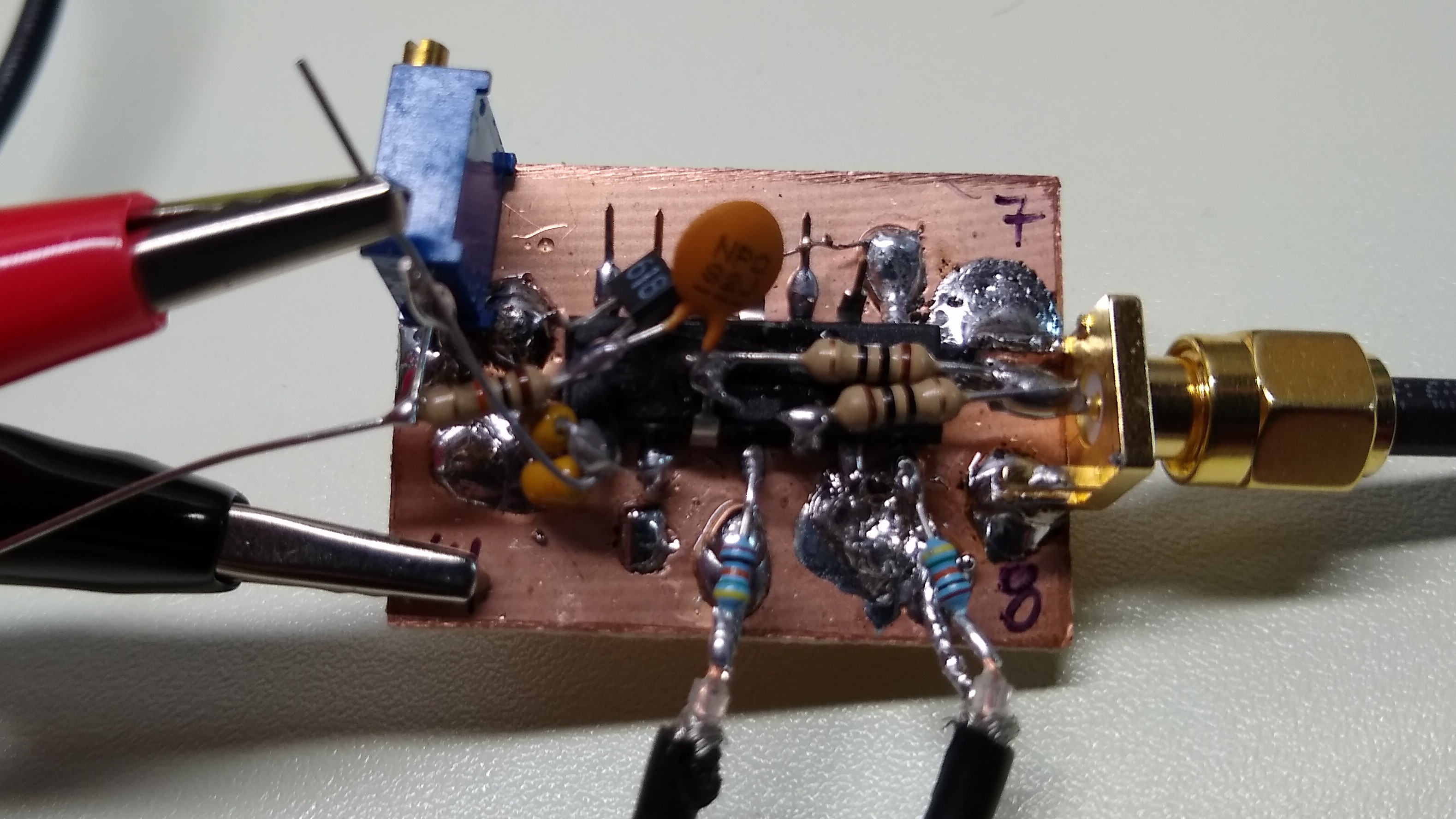
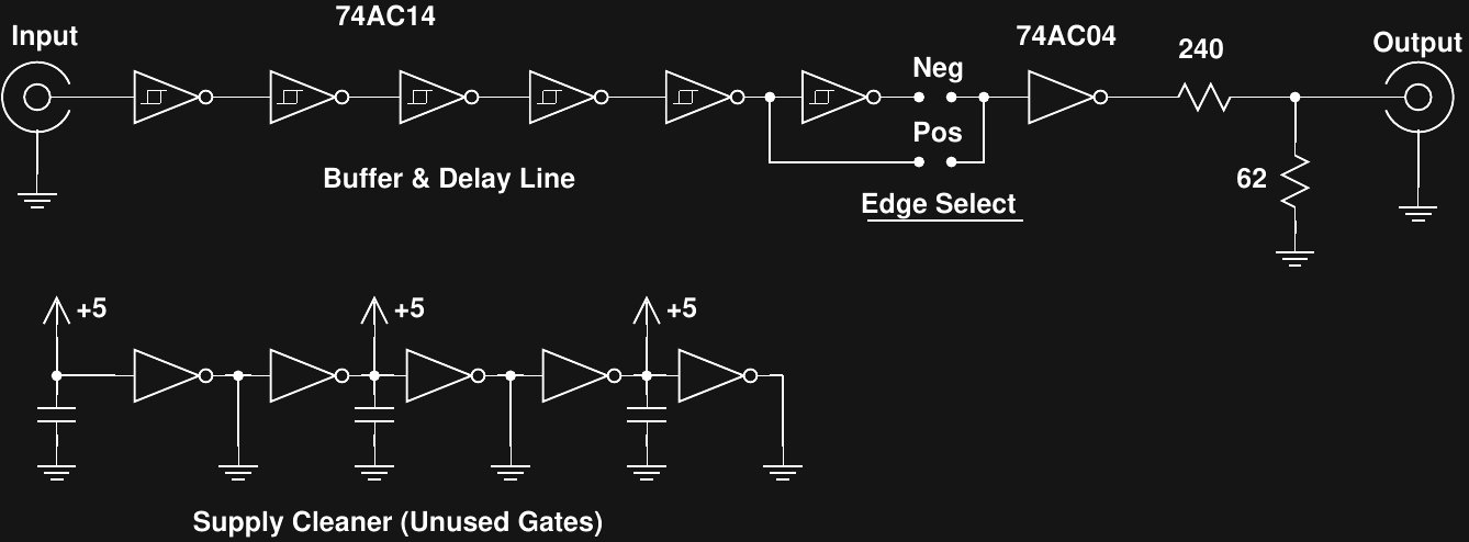
02/09/2019 at 03:54 • 0 commentsThis is the first in a few logs to document everything that went into getting the first sampling head to work. I needed a new edge generator with a build-in delay to line up the pulse edge with my sweep delay generator (details next log). I ended up making this with a 74AC14 and 74AC04.
![]()
The 74AC14 chain delays the input pulse, and you can select the polarity by choosing the output tap. One section of a 74AC04 is the output buffer/driver, and there's a resistive divider to provide a source-terminated 500 mV output into a 50-ohm load (100 mV unloaded). With the unused portions of the 74AC04 I made a "supply cleaner." This just connects unused *outputs* of the gates to Vcc and GND to essentially add more supply pins to the package. The MOSFETs in the output structures of those gates have a decently low impedance and hopefully help with the notorious supply problems of the 74AC family.
![]()
I measured the output of this new circuit with a few scopes, including the new sampling head.
1 GHz Tektronix TDS-784D
(It's a modified TDS-754D, but don't tell anyone :-)
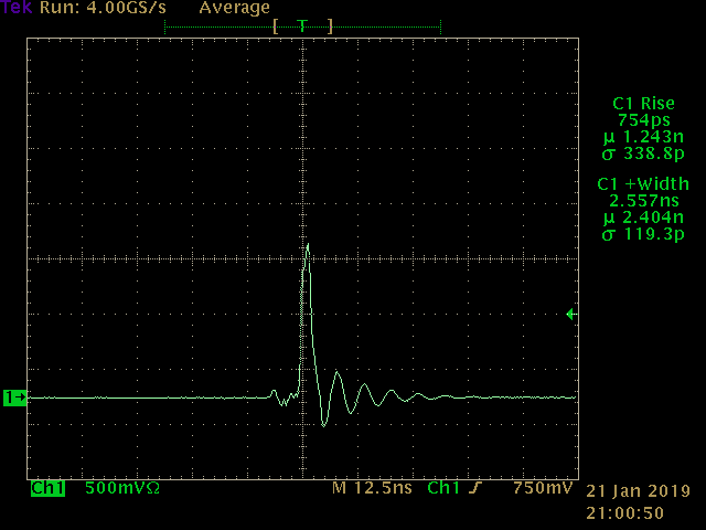
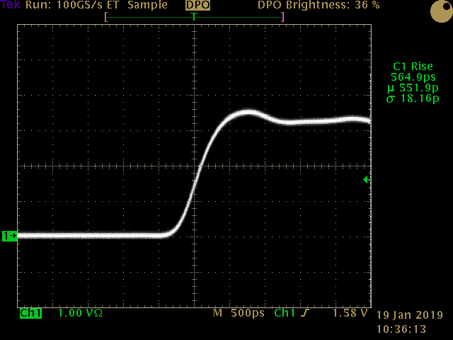
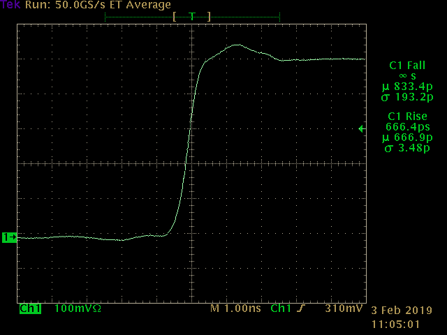
Here's the rising edge of the pulser on a 1 GHz scope. It looks pretty good except for a little bump about 1 ns after the edge. This isn't a reflection: there's not enough space anywhere to produce this timing. I think it's the 74AC04 itself. In any case, it's a feature on a short timescale that we can use to check other scopes. The rise time of the edge is 667 ps, not counting the contribution of the scope itself (it's likely under 600).
![]()
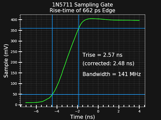
1N5711 Sampling Head
(It's a homebrew sampling head, tell anyone you like :-)
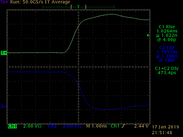
I painstakingly collected data for this edge using the same setup as before. It ended up being 97 points total, averaged over millions of input pulses. The calculated rise time for the sampling gate is 2.48 ns, for a bandwidth of 141 MHz. This is close to the 155 MHz I previously estimated with the fall time of a different pulse.
Interestingly, the little bump at the top of the pulse is just barely visible. I think this "scope" just doesn't have quite enough bandwidth to show the bump.
I'll come back to this image in a later log. There's a lot going on to capture this data.
![]()
300 MHz DS3202A
(It's a modified DS2072A, but don't tell anyone :-)
This 300 MHz scope has just enough bandwidth to start to render the bump at the top of the pulse.
![]()
100 MHz DS1104Z
(It's a modified DS1054Z, but don't tell anyone :-)
On a 100 MHz scope, there's no bump on the pulse at all.
![]()
Conclusions
It certainly seems to behave like a 140 MHz scope - the captured waveform looks better than the 100 MHz commercial scope and worse than the 300 MHz model. So far, so good.
-
Yay! It's an Oscilloscope
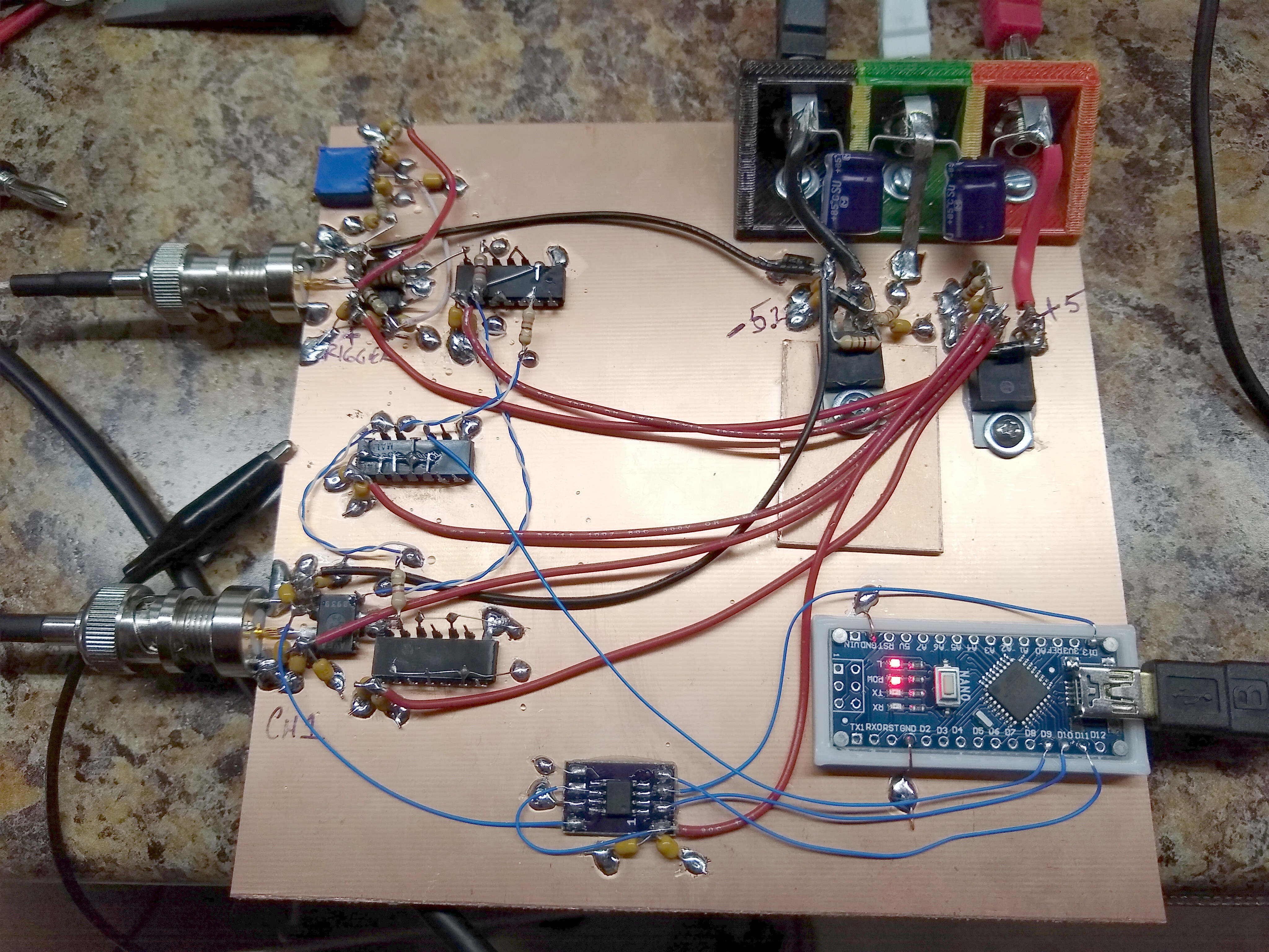
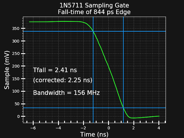
02/03/2019 at 04:38 • 3 commentsIt was a long day in the lab, but I got it working. There are actually four oscilloscopes in this picture: three commercial ones, and one homebrew version on those copper clad boards. Right now, it has the most primitive interface you can imagine - you turn a 20-turn potentiometer to set the time at which you want to sample the input waveform, then read the voltage at that time off a voltmeter. But, even with this insanely stupid interface, it still has a higher bandwidth than the DS1054Z at the back of the table. I measured the bandwidth of the new sampling scope at 156 MHz. Not bad for a first "toy" version.
![]()
There are a lot of things to document, and it will take a little while to get it all down, but in a nutshell, I made an adjustable time delay for the x-axis that allows you to move the sample trigger pulse by about 10 ns, with resolution of maybe 30-40 ps (limited by jitter). Using this, I was able to capture a trace of the fall of a 844 ps pulse edge. The 90-10% fall time is 2.41 ns, but correcting for the fact that the input has a fall-time of 844 ps yields a 2.25 ns fall time for the sampler itself. Using the old 0.35/t rule, this front-end has a bandwidth of 156 MHz.
![]()
This plot was created from 79 data points taken by hand. For each one, the delay time was adjusted slightly with the potentiometer, then the voltage was read from a voltmeter. I wrote all the points down on paper. Because of the slow data collection, there's an insane amount of averaging going on. The pulse had a frequency of 1 MHz, and assuming it may have taken me 10-15 seconds to collect each point, there could be 10 million samples averaged to get this result. That's why you don't see any noise.
I think I'll have to automate this before the next test.
![]()
Next Up
I have to document the variable delay and pulse generator used to capture this data. But right now I'm tired and am going to sleep.
-
A Toy Diode Sampler
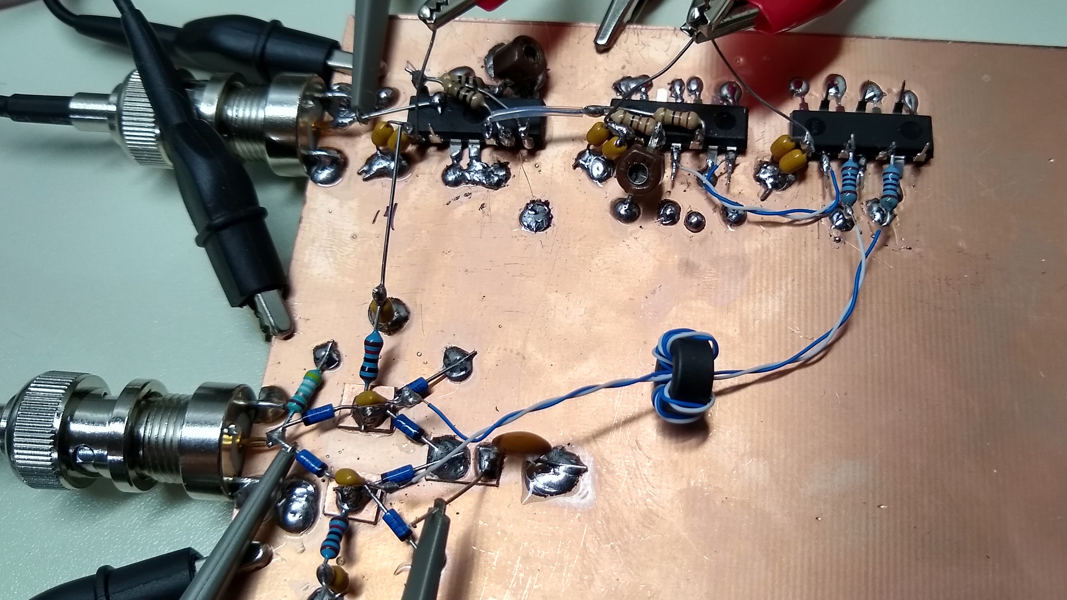
01/29/2019 at 04:12 • 0 commentsOne of the ways forward on this project is using diode sampling gates. Schottky diodes that can switch well into the tens of GHz are readily available, so it's just a matter of connecting them to the right stuff :-) I started out with a toy version - not that the 1N5711 diodes aren't capable, but the layout and pulse generator limit the circuit to lower frequencies.
![]()
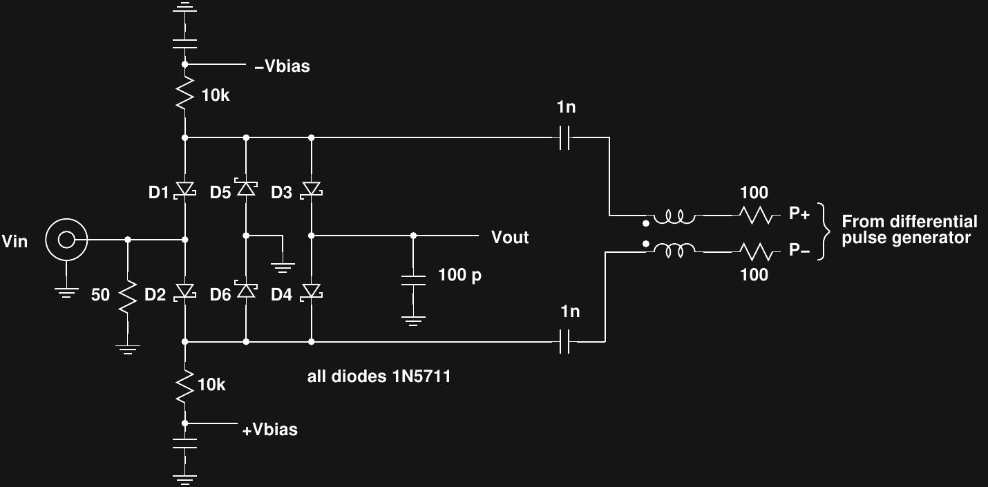
The business end of the sampler uses six 1N5711 diodes: four in a bridge, and two to clamp the reverse voltage.
![]()
In the real thing, you'd use matched pairs (or quads) of diodes in SMT packages, but these work OK for breadboarding. I selected the six diodes from a lot of 50 by choosing ones that had about the same forward voltage. D1-D4 form a sampling bridge which is biased on during the brief sampling pulse. Between pulses, D5 and D6 clamp the voltage on the bridge to enhance isolation between the input and output. Ideally, these would be biased with split supplies, but for the initial tests, I left the bias supplies disconnected.
During the sample pulse, the 100 pF output capacitor sees the input voltage through the forward-biased diodes in the bridge and charges toward the voltage. The RC time constant of the circuit is based on the input impedance of 25 ohms (50 ohm source impedance in parallel with the termination) and maybe 10 ohms through the diodes. Combined with the 100 pF capacitor, this is around a 3.5 ns time constant. It doesn't matter that the capacitor doesn't charge fully during the strobe pulse, so this RC time constant doesn't set the front-end bandwidth. We can sample the waveform at the same point repeatedly until the capacitor settles to whatever resolution we need. This also does a lot of noise reduction by averaging.
I am also considering using a buffered version of the output voltage to boostrap the midpoint of D5/D6 instead of grounding it. You see this in some sample and hold architectures, but I'm not sure it's entirely needed yet.
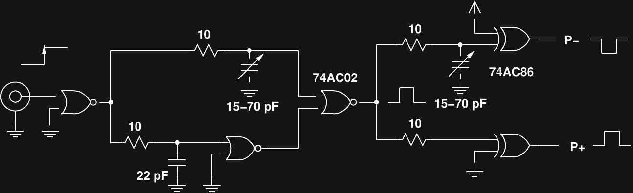
The differential sampling pulse comes from a previous log, repeated here for convenience:
![]()
The rising edge of the input pulse creates a brief (approx. 2 ns) differential output pulse. A 2 ns sample pulse should create a sampler with around 200 MHz of bandwidth, although I haven't been able to test it that far yet.
Initial Tests
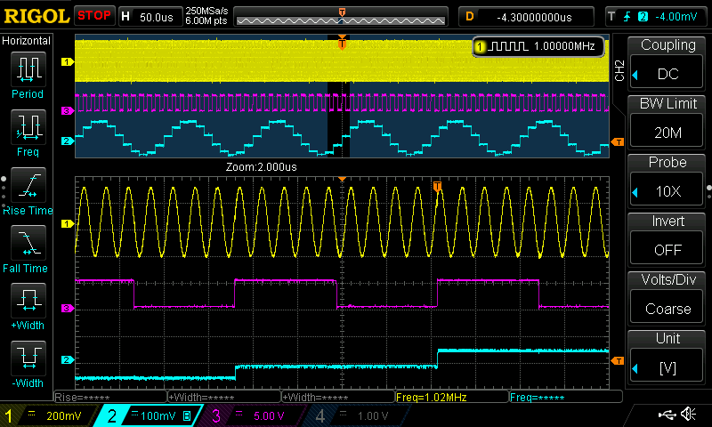
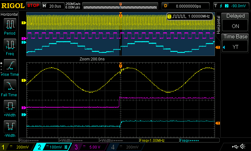
I was able to test the sampler using two outputs from a DDS signal generator: one output is the signal to sample, while the second output generates the sample clock. Here's an example of how it works:
![]()
The yellow trace is the input waveform: a sine wave in this case. The magenta trace is the sample clock. At the rising edge of the sample clock, the input voltage is sampled and stored on the capacitor (cyan trace). You can see in the upper traces that the output is a "slowed-down" version of the input, since the sampling clock has been chosen to be slightly longer than 1/10 of the input period. In a real system, a trigger circuit and delay generator would create the sampling clock.
In the expanded traces (bottom), you can see how the output voltage changes in steps at each edge of the sample clock.
Sampler Kick Out
In this image, you can see the sampler "kick out," or perturbation of the input signal that happens during the sample pulse (lower yellow trace, directly under the trigger marker). This pulse feeds back into the measured system, which can be problematic. However, this kick-out can also be used to characterize the impulse response of the sampler. This may be useful later on.
![]()
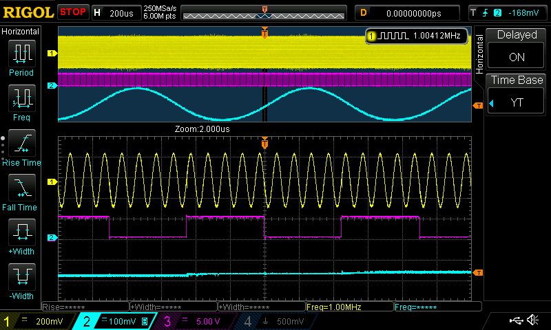
More Resolution
From the above figures, it would be easy to mistake the sampling quantization with amplitude quantization and assume only coarse output steps can be created. This is not true; the examples above are simply to illustrate the behavior of the sampling gate. With a different sampling rate, a high-resolution version of the output emerges.
![]()
Output Offset
If you look carefully at the upper cyan traces in these images, you can see that two of them have a DC output offset. These were captured without the common-mode choke in the sample line. It turns out that the kludgy differential pulse generator doesn't create very symmetrical pulses, so there is a common-mode pulse along with the differential. This common-mode pulse gets rectified by the diodes to create a DC offset on the output. The solution is a transmission-line transformer made by wrapping the twisted pair line a half dozen times through a type 43 ferrite core. This common-mode choke allows the differential component of the pulse to pass, while blocking the common-mode pulse. The result is a zero-centered output.
This was a lucky guess on my part, but adding the transformer worked like a charm.
I probably should also add a manual offset adjustment. Every sampling gate circuit in old oscilloscope manuals seems to have one.
Next Steps
I have a PCB version of a similar circuit I actually build a few weeks ago, but never got working quite right. Now, having seen a diode sampler work, it's time to go back and debug that board.
It's also time to see if CML or PECL differential outputs have enough swing to turn on the diodes in this sampler.
-
Fun with Clip Lines
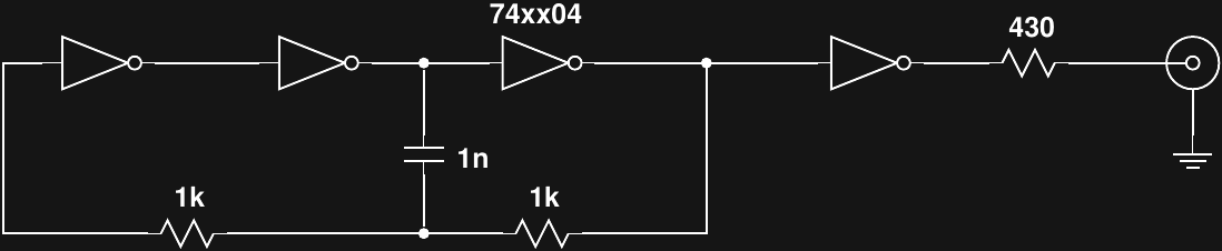
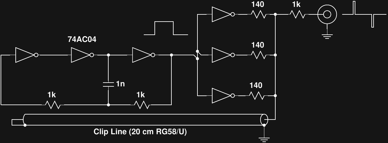
01/22/2019 at 03:23 • 0 commentsIf you dig through enough schematics for old Tektronix sampling heads, you eventually come across "clip lines." The idea is to use a stub section of transmission line to shape fast pulses. To play around with the idea, I threw together a test using another 74AC04.
![]()
The circuit uses three of the inverters in the package as an RC oscillator with the remaining three paralleled through resistors to create an approximately 50 ohm driver. Three gates can't really supply enough current for use like this - you need four - but it was good enough for a quick test.
The clip line itself is a 20 cm section of RG58/U cable shorted at one end. When the output drivers go high, the line initially looks like a 50 ohm resistor (its characteristic impedance), and cuts the output amplitude by half, forming a divider with the 50 ohm output impedance. The edge of the pulse travels the length of the line, is reflected with inverted polarity by the shorted end, and returns to combine with the output. Since the reflected signal was inverted, it cancels with the driver voltage, leaving a zero output. So, the output pulse is only high for one round trip through the cable, creating a predictable, repeatable, and stable output pulse width.
![]()
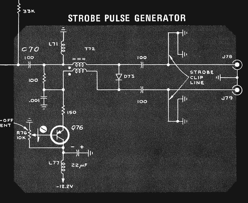
Here's how Tektronix used them in one of their samplers: the clip lines control width of the pulse created by the step recovery diode, D73. The whole thing looks awesomely simple.
![]()
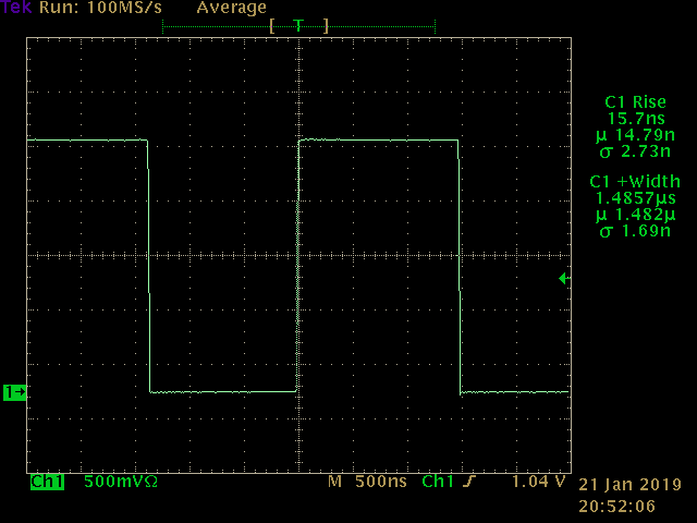
No Clip Line
The output of the pulse generator without the clip line attached is a 5V square wave with 1.48 us (yes, microsecond) positive pulse width. The rise time measurement is inaccurate at this timebase setting. The voltage scale is also wrong, since I forgot to adjust for the 20x attenuator.
![]()
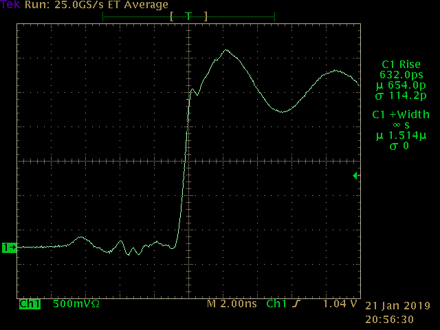
Zooming in, we can see the edge is very fast, and there's some ringing at the top of the pulse.
![]()
Now, with Clip Line
Adding the section of transmission line to the circuit transforms the output waveform into a short pulse, in this case around 2.5 ns wide. I measured the section of RG-58U cable to be approximately 20 cm long. With a velocity factor of 0.66, this should be 1.01 ns one-way, creating a pulse width of 2.02 ns. That's close enough to the measured value to be convincing - after all, the pulse isn't particularly pretty, and I don't know exactly where the scope is measuring the width.
The amplitude is also halved to 2.5 V (again, the attenuation setting on the scope was wrong).
There is also a corresponding negative pulse at the falling edge of the input signal. The scope couldn't show both on the screen at once because they are too narrow relative to the spacing.
![]() There's some ringing at the end of the pulse, probably because my quick test circuit doesn't present a good 50 ohm output to match the Z0 of the cable. This causes reflections of the initial edge to bounce around until they finally decay.
There's some ringing at the end of the pulse, probably because my quick test circuit doesn't present a good 50 ohm output to match the Z0 of the cable. This causes reflections of the initial edge to bounce around until they finally decay.![]()
Conclusion
Hey, this kinda works. Maybe I should really concentrate on getting a fast, clean step and let sections of transmission line form my pulses.
-
CMOS Differential Pulse Generator
01/21/2019 at 04:53 • 0 commentsSo, I combined a few ideas from previous logs and prototyped a differential pulse generator with 74AC CMOS gates. The goal is to have a differential output with large swings for short pulses. I got it to 10V swings and around 1.6 ns pulses.
![]()
There are two parts to the circuit: an edge-to-glitch converter and the XOR differential stage from previous logs. Both have capacitive trimmers for fine adjustment. I got smart and grounded the correct side of the trimmers this time, so they can be adjusted with a metal screwdriver without affecting the circuit.
![]()
With some careful tuning of both trimmers, I ended up with the output shown below. Ch1 (green) is the output of the upper XOR, it swings from 5V down to 0 for the pulse. Ch2 (blue) is the lower XOR output; it swings from 0 up to 5V. The magenta/pink traces are math combinations of the two. The magenta trace is the sum of the two outputs - ideally, it should be a constant 2.5 V; any wiggles are errors in the two outputs. The pink trace is the difference between the two outputs - the differential signal. It's not a bad pulse, really. It is 1.6 ns wide, and has an amplitude of about 10V. With the 24 mA output capability of the 74AC gates, it should have no problem driving a diode sampling gate through relatively large resistors (perhaps a few hundred ohms).
Note how a lot of the ringing on the upper and lower pulses have cancelled in the differential pulse. That's a neat side effect that I hadn't anticipated.
This is probably OK for a first test, although I'd really like to be able to do this at least 3x faster. 74LVC1G gates might come close.
![]()
-
Some Edge Tests
01/19/2019 at 16:44 • 4 commentsI finally populated a couple of PCBs I designed about a month ago. These are simple Schmitt-trigger oscillators with 74xx1G04 inverter output buffers. I populated one with 74LCV1G devices and one with the faster SN74AUC1G to compare the edge rates - the results were surprising.
![]()
The circuit is shown below. I didn't populate one of the inverters intended to drive a sync output. The output series resistor is 453 ohms, creating a 10x divider when used on a scope with 50-ohm input termination. An SMA-BNC adapter lets you connect the board right at the scope input with no intervening cable to slow the rise time.
![]()
ADCMP606
As a baseline, I re-measured my ADCMP606 version. This uses a CML-output comparator with typical datasheet rise times of 160 ps. On my 1 GHz scope, it measures 392 ps, which is more the scope than the pulse. For the rest of the measurements, I'll assume the ADCMP606 is actually creating pulses with 160 ps rise time, so the scope's rise time is sqrt(392^2 - 160^2) = 370 ps. This estimate is probably high based on some other clues, but I'm going to stick with it for now.
The output here is 400 mVp-p (single-ended CML), and shows very little overshoot. The estimated slew rate is 2 V/ns.
![]()
74LVC1G04 (@ 5V)
I populated one PCB with 741GLVC parts. The rise time displayed on the scope is 485 ps. After correcting for the (estimated) scope's rise time, this becomes sqrt(485^2 - 370^2) = 314 ps. This sounds low and probably is, but is useful for comparison with the other devices. Also note the ringing after the edge. Although the rise time is longer, this is a 5 V pulse as opposed to the 400 mV from the CML part, so the slew rate is around 12 V/ns - 6x faster!
Note that this trace appears faster because the timebase is different. The scope uses an amplitude histogram of the waveform to determine the 10% and 90% thresholds, and it can be thrown off by the overshoot. By expanding the timescale, you can include enough of the steady-state high output to stabilize the histogram and produce better measurements.
![]()
SN74AUC1G04 (@3.3V)
I pushed these parts to their max voltage for this test. The measured rise time is 552 ps, which might be as low as sqrt(552^2 - 370^2) = 410 ps. Either way, the rise time on the SN74AUC parts is slower than the 74LVC1G. This is surprising, because the AUC part is much faster than the LVC, with a 1.6 ns max Tpd (2.5 V) vs 3.1 ns (5 V). The output also shows less overshoot. These effects are probably due to the special output structure of the AUC gates, which is supposed to eliminate many of the reflection problems on high-speed boards. You can supposedly drive 15 cm traces without source termination resistors.
For reference, the estimated slew rate is 6.4 V/ns, a little more than half that of the LVC part.
![]()
74AUP1G04
I have some 74AUP1G04's around somewhere - these are low-power devices with longer Tpd (4.2 ns max into 15 pF at 3.3V). I can't find them at the moment, but I have one PCB left for when I do. I'll update the log when (and if!) I can ever locate those parts.
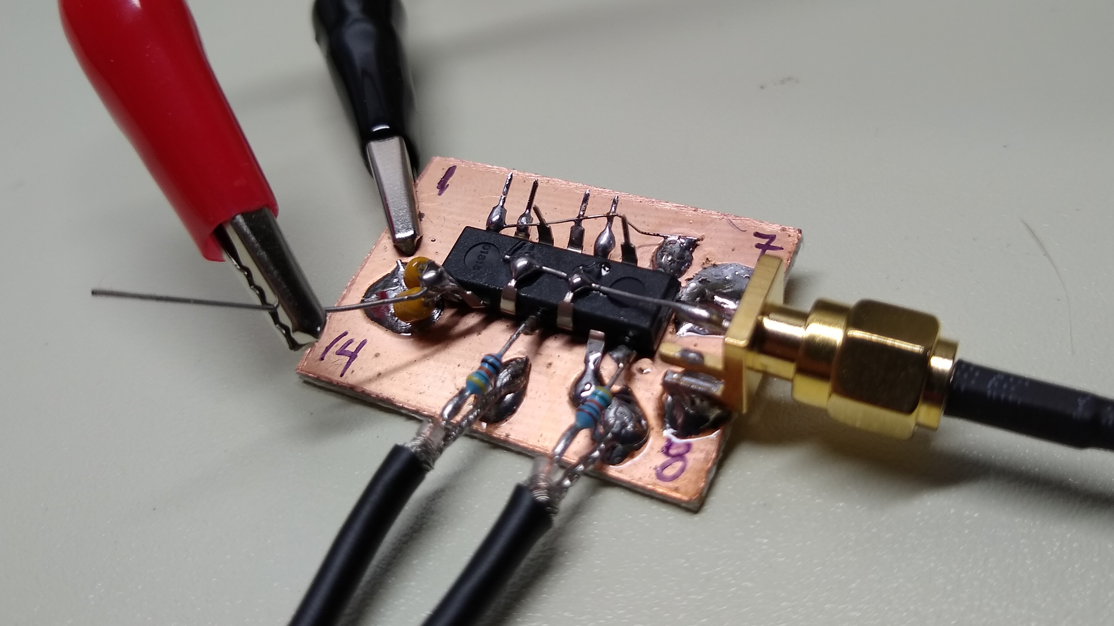
74AC04
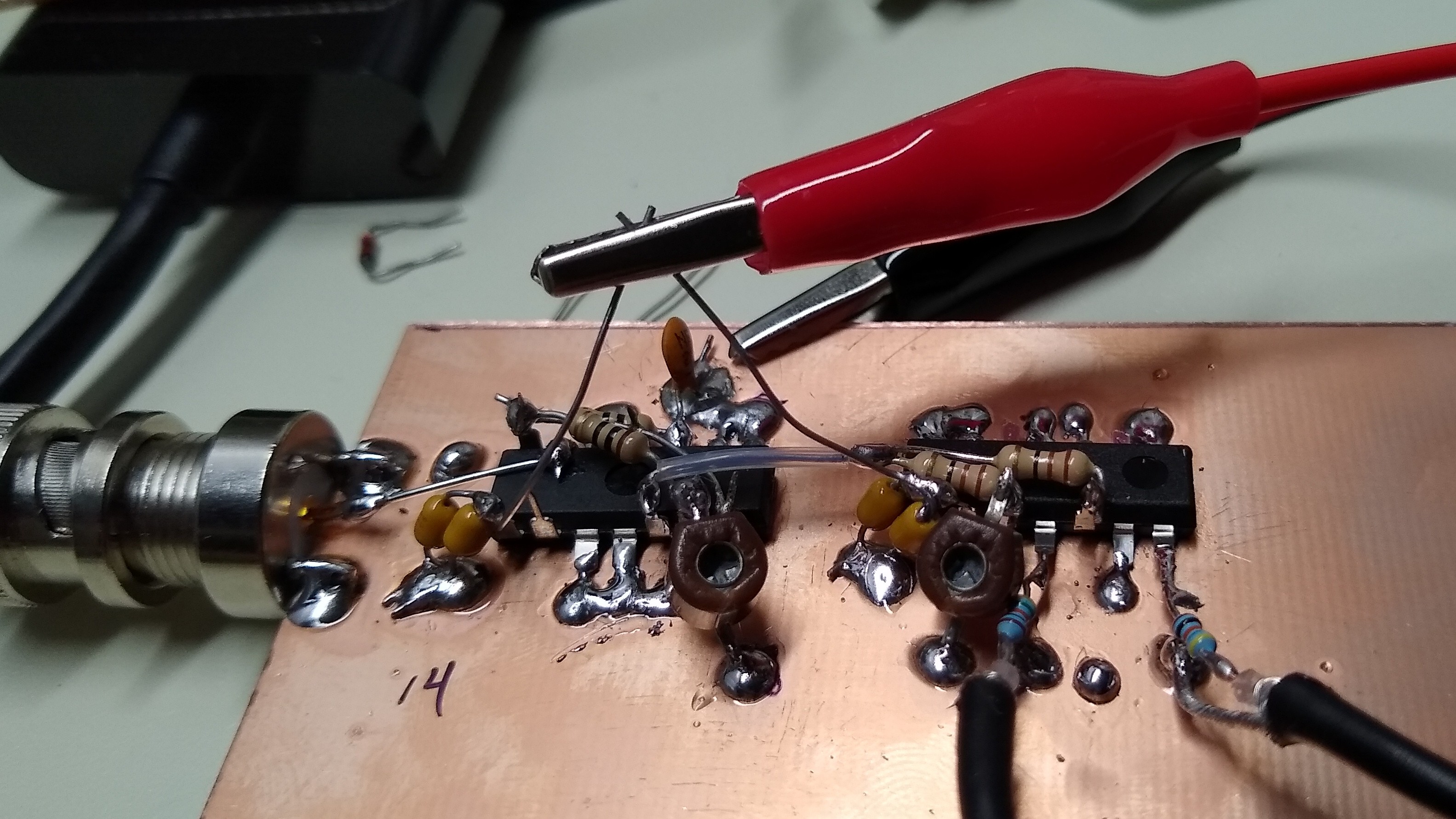
I still can't find the 74AUP1G04's, so I decided to try some DIP parts. I realized that I has never tested a 74AC gate right at the scope input before - there had always been some cable in between. So, this time, I built a pulser right next to a BNC male plug.
![]()
This circuit is a 3-inverter RC oscillator followed by an inverter-as-buffer. I used a 430 ohm output resistor because I was too lazy to look for the 453's. It's a 9.6x probe :-)
![]()
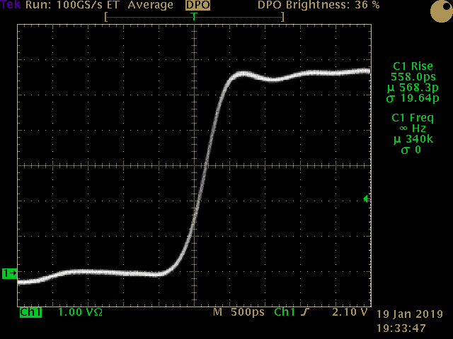
When measured this way, the 74AC04 shows a 568 ps rise time. This would be 431 ps correcting for the scope response as I did above. I had always measured something more like 1 ns when testing through cables. This really makes me want to investigate a little more about exactly what the difference is. Maybe I have an adapter so I can try interposing some different length (and type) cables between this board and the scope.
![]()
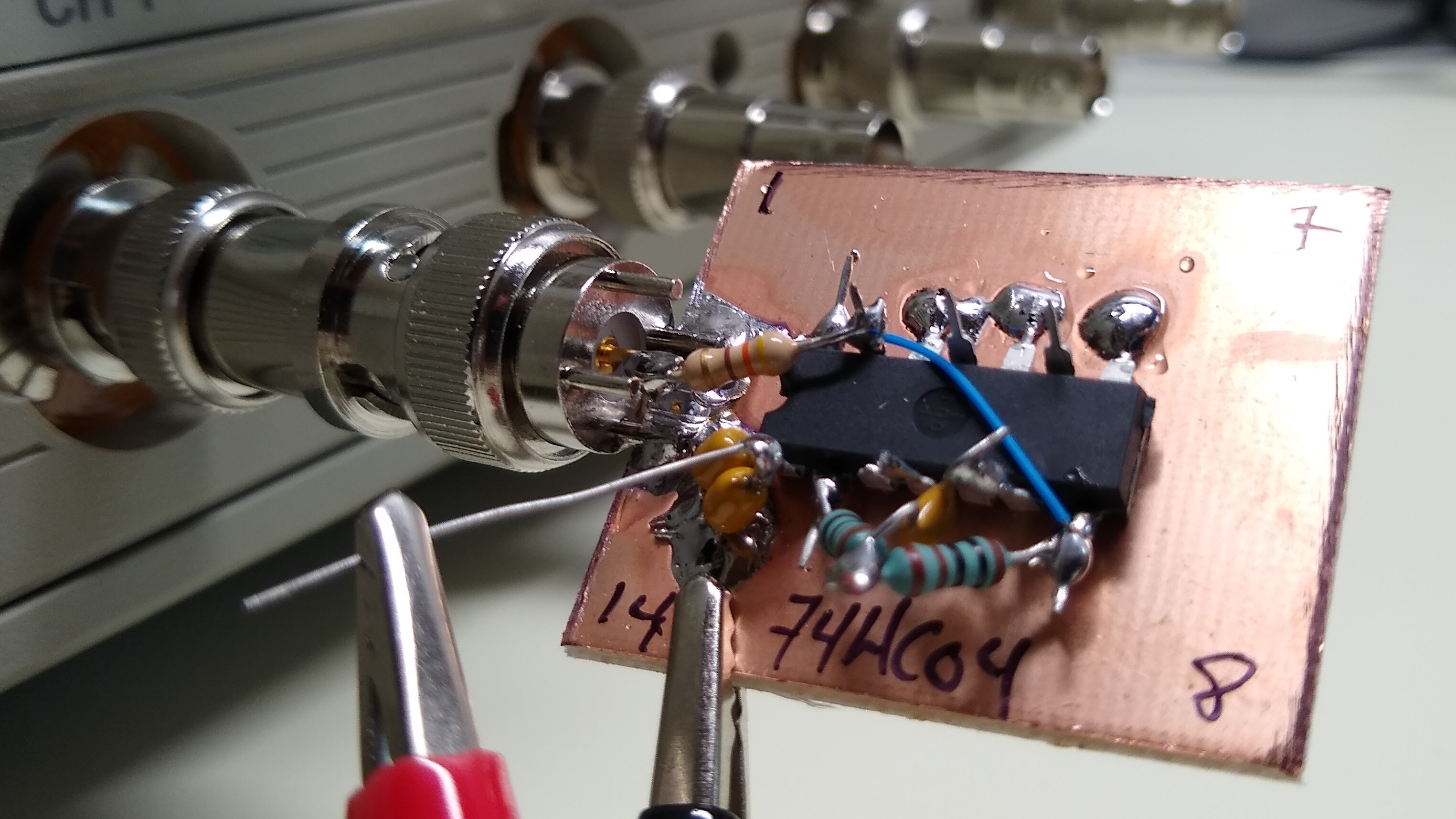
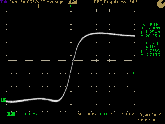
74HC04
While I was at it, I threw together the same board using a 74HC04.
![]()
The circuit is the same, except with for the HC logic IC. The measured rise time is 1.25 ns (1.19 corrected). That's around 2.75x slower than the AC, which seems about right.
![]()
Conclusions (?)
None of these rise times were tested under any significant loading. The 10x resistive probing arrangement I used should present negligible capacitance, so the rise times when driving anything significant would be longer (maybe much longer).
-
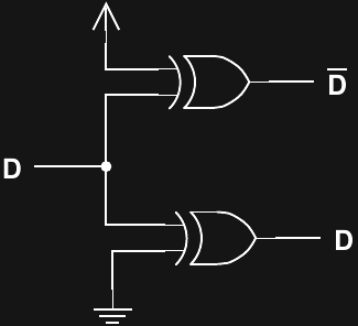
XOR on the Bench
01/18/2019 at 03:15 • 2 commentsIn the last log, I speculated about using a pair of XOR gates to get a complementary (differential) pair of outputs from CMOS logic. This brought up a lot of questions, and the best cure for that is some quality bench time. I threw a 74AC86 XOR package on some copper clad and tested it out.
![]()
It's the same idea from the last log: use two XOR gates, one as an inverter, one as a pass-though, and hope that the skew between the two outputs is low.
![]()
The output shows around 570 ps of skew. Compared to the 1 ns rise/fall times of the signals, this isn't really very good.
![]()
I wasn't sure how much this skew was due to differences between the individual gates, or to the different delay when used as an inverter (as predicted by @salec ). To test this out, I swapped the gates around, and measured around 470 ps of skew. A little algebra convinced me that this means there's 50 ps difference between the two gates themselves, and around 520 ps difference due to using one of them as an inverter.
![]()
520 ps skew on a signal with 1000 ps edges ain't great. But, in absolute terms, this is small enough to "tune away" with a potentiometer or other adjustable delay, as suggested by @Yann Guidon / YGDES.
EDIT
Sleep is over-rated. I tuned this thing instead. I added two 10 Ohm resistors and a 15-70 pF cap. With some careful adjustment, I reduced the skew to 2.6 ps! It's not very stable at that value, but it seems to stay in the single digits to teens. A skew this low is kind of meaningless when you consider that the difference in rise and fall times is around 70 ps. I think the conclusion is that you can, indeed, just tune this thing until it works.
![]()
For completeness, here's the new circuit.
![]()
The trimmer is difficult to adjust - the only tools I have that will fit in there are metal screwdrivers, and they add their own capacitance to the circuit. You have to over-compensate so that when the screwdriver is removed, the circuit ends up tuned. It takes a few tries. Maybe I need to print some alignment tools?![]()
The probes deserve a mention, too - these are simply 453 Ohm resistors soldered on to the end of a length of RG174 cable. Combined with the scope's 50 Ohm terminators, they make 10:1 probes with a decent bandwidth, much better than commercial probes I can afford. To make these two, I just cut a cheap BNC cable in half - as close to exactly half as possible to maintain equal delays.
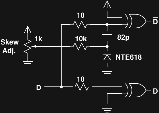
EDIT 2019-01-19I read in "High Speed Digital Design: A Handbook of Black Magic" about using varactors to tune logic delays. I had a selection of 10 different types of varactors in the diode bin, and chose an NTE618 for a test - this is a device originally designed for AM tuners. It has a wide capacitance range 20-460 pF, although you need up to 15 V reverse bias to push it to low values. I put it in series with an 82 pF fixed cap, and biased it through a 10 K resistor and a voltage divider.
![]()
It's the same idea as the trimmer cap version, but now electronically tunable.
![]()
With the components used, the tuning range is around 310 ps. This is enough to fine-tune the delay if you can get it in the ballpark first. The varactor drifts with temperature, though, so some kind of automatic calibration that could periodically adjust it would be nice.
This is probably overkill for the planned use, but an interesting experiment nonetheless.
-
What am I missing?
01/16/2019 at 12:42 • 11 commentsSo, I'd like to find a CMOS logic gate with complementary outputs - you know, like ECL, CML, LVDS, or any of those differential signaling families. It's not for a logic application; it's for driving a diode sampling gate with a truly differential pulse - transformers just aren't cutting it (story for another log!). I don't think such things exist, so I came up with this. Can I do better? What do you think?
![]()
I'm hopeful that if I use two devices from the same gate package, I can get a small timing difference (skew) between the two outputs. I'm looking at the 74LVC2G86 right now, because I need the large voltage swings afforded by a 5V supply and the 32 mA drive.
I had considered somehow using the Q/Qbar outputs of a d-flip-flop, but I think there are a few problems with that.
-
Stroboscopic Converters as Sampling Oscilloscopes
01/11/2019 at 21:54 • 0 commentsI just prototyped a stroboscopic A/D converter. It works, and it appears that you could make a similar one with available parts that would function as a 10 GHz sampling oscilloscope. This is where it gets interesting, people.
![]()
This version won't do anything near 10 GHz, but works as a proof-of-concept, and I was able to build it with parts I had on-hand. I love that kind of project.
Stroboscopic Converters 101
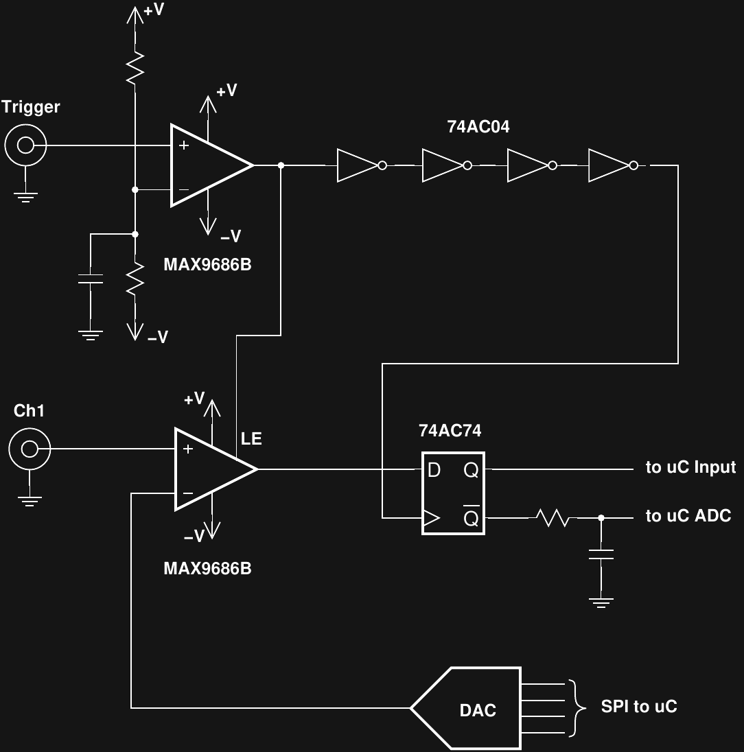
A stroboscopic converter looks a lot like a successive-approximation ADC (SAR ADC). If you consider just the DAC and lower comparator in the figure below, you can see the elements of a simple SAR ADC. Assume for the moment that we apply a DC voltage to the Ch1 input. We can read the value of that voltage by successively comparing it to different voltages output from the DAC. A naïve implementation would simply scan through all possible DAC output voltages, taking at most 2n tries for an n-bit DAC. You can do much better than this using a binary search over the DAC levels, of course, taking only n tries. SAR ADCs are cheap and accurate for low- to medium-speed ADCs, so are seen in many commercial offerings.
We've made a voltmeter. Now we need to turn it into an oscilloscope.
![]()
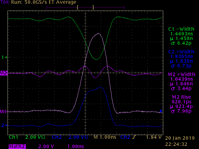
A closer look at the lower comparator reveals a latch-enable input (LE), allowing the voltage to be compared at a specific instant in time. To digitize an AC signal, a trigger pulse enables the lower comparator repeatedly at the same point in the waveform cycle. At this point, the motion of the input signal has been frozen, as if by a stroboscope, and the SAR conversion can proceed as normal. Once that particular data point has been digitized, the trigger point is moved slightly in time, and a new data point is captured. Doing this repeatedly results in a set of voltage measurements vs time, which is exactly what an oscilloscope does.
The schematic is a bit simplified and differs from what I actually built. For example, I needed 74ACT parts, since the comparator output is TTL level, which can't drive 5V CMOS inputs. All I had were 74ACT14's, so those went in for the 74AC04.
More importantly, a variable trigger delay is missing from the diagram. This part is critical to be able to reliably sample the input signal at specified points in time. In the prototype, the time scanning is faked by generating appropriate trigger points with arbitrary waveform generation software. For a real system, a variable delay line will need to be implemented. Luckily, such parts are made for very fine timing adjustments to critical clock and data lines. For around $10, you can obtain a digitally adjustable delay line with 10 ps steps (and an analog fine tuning input). The delays will need to be calibrated for use in a sampling scope, but that's an issue for another time. I'm working on a prototype adjustable delay board now.
First Tests
I haven't finished an adjustable delay line yet, so I used two outputs of an FL2k USB-VGA dongle with the osmo-fl2k software to generate both the sampling trigger pulses and a test sine-wave input. That's what the arbitrary waveform generator from the previous log was all about.
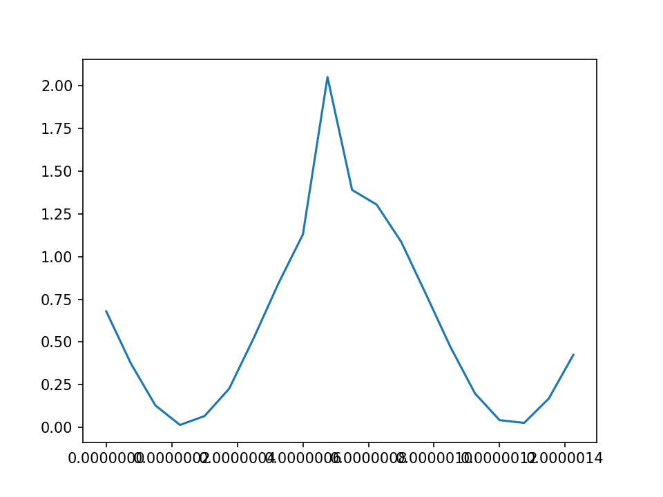
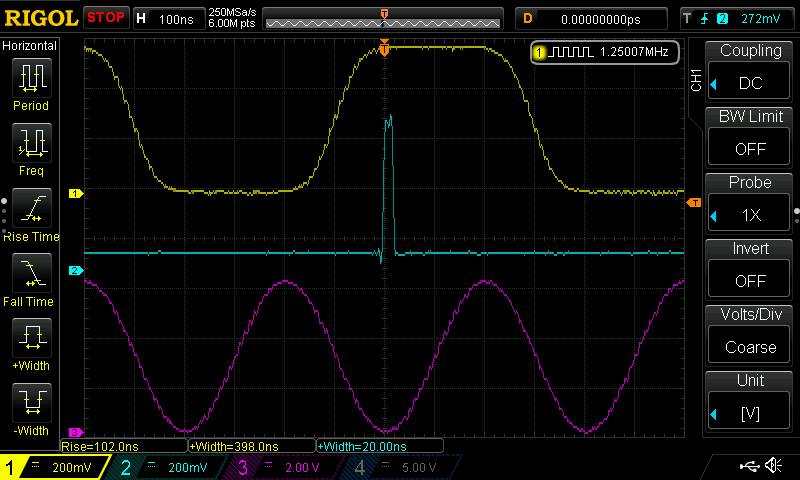
I managed to get a decent first result, sampling a sine input every 67 ns.
![]()
You can see where the successive approximation routine got stuck and produced a bogus conversion - clearly, there's a bug somewhere. It's not a bad first try, though. Now to go faster and faster and faster and...
References
This has been done before. A kickstarter from 2013 promised a 10 GHz sampling scope for $300, but didn't get funded. The clever folks over on eevblog eventually recognized this as a stroboscopic converter design, with an older version using ADCMP582 comparators (8 GHz input bandwidth). That design wasn't open-source, and appears to have been lost, so it makes sense to re-invent the (free) wheel in this case.
Next Steps
I'm still experimenting with a more traditional diode sampling gate. The difficulty is in generating the sampling current pulse needed to turn the gate on for a short sampling period. Modern parts can generate very sharp edges, but offer only small voltage swing, engineered to reduce EMI. This reduced swing has difficulty turning on the Schottky sampling diodes, though. Traditional diode sampling gates used step recovery diodes (diodes again!) to generate the pulses. Step recovery diodes are still available, but border on being unobtanium, so I'd like to avoid them if possible. More research is needed.
I'm going to pursue the stroboscopic converter angle in parallel with the diode sampling approach. There are a few faster comparators on the market which could get the bandwidth up to 10 GHz. Unfortunately, these are very expensive, so I will probably take an intermediate step, shooting for maybe 1 GHz bandwidth at first.
-
Tangent #0: Arbitrary Waveform Generator
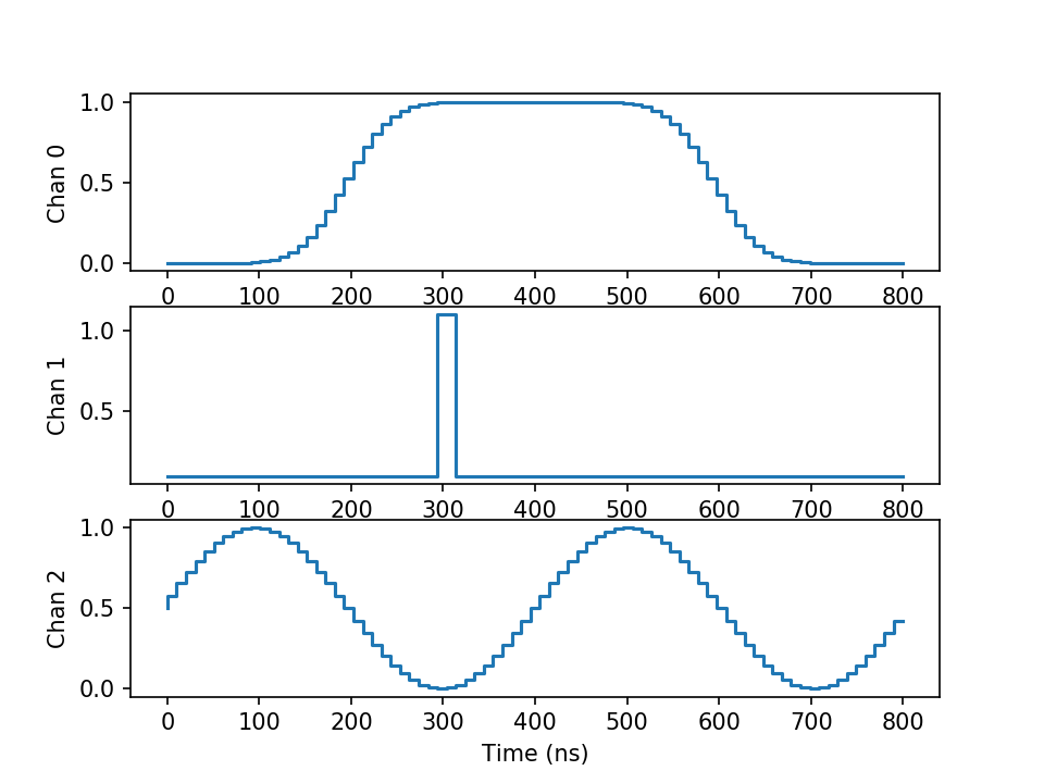
01/02/2019 at 00:41 • 0 commentsWhile considering my next move, I thought it would be useful to have a simple multi-channel arbitrary waveform generator. The first thing to come to mind was the FL2k USB-to-VGA dongle and osmo-fl2k software library. I put together a python module for defining and digitizing some interesting waveforms which can be output through the adapter. The example code in GitHub generates the following waveforms:
![]()
There's no filtering on the output of the FL2k dongle (yet), so the waveforms look a little rough. There's some OK documentation of how to use the code on the GitHub page. As shown above, you can define sine waves, Gaussian edges and pulses with defined edge rates, and square-sided pulses. You can also define linear edges (ramps) and exponential (RC) edges. You can define the rise and fall times and the high and low measurement points (default 10% and 90%), as well as the edge threshold (default 50%). The rise times and pulse widths measured on the scope are very close (modulo noise) to those defined in the code.
You choose the sample rate, and the code allows you to preview the output.
![]()
The outputs from the FL2k aren't very fast, in this case only using 100 MS/s (my laptop will do 150 MS/s maximum with this hardware). But, I think I need a source of some lower signals for initial testing before I move to shorter timescales.
The Rise and Fall of Pulses
A project in which I try to go faster and faster


 There's some ringing at the end of the pulse, probably because my quick test circuit doesn't present a good 50 ohm output to match the Z0 of the cable. This causes reflections of the initial edge to bounce around until they finally decay.