 ELECTRONOOBS
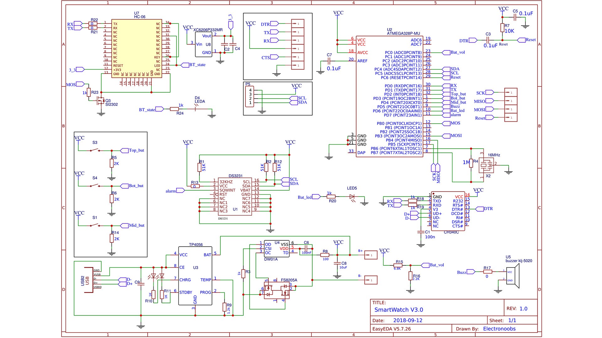
This board has a lot of components. After you solder the PCB and make it work, it will ahve all the specs below:
- USB charging circuit (3.7V battery protection)
- LOW power consumption
- Battery voltage read
- USB programming chip (CH340)
- UART programming (extra)
- RTC (real time clock) and get:
- Day of the week
- Date: day, month, year
- Temperature
- Set alarm interruptions
- Buzzer control
- LED control
- 3 Push buttons
- Bluetooth connection (UART communication)
- OLED dispaly (i2c communication)
Below you ahve the full schematic of this PCB so you could know each value for the resistors and capacitors adn also the name of each component. There are a lot of components so go slow when soldering. Below you ahve a step by step on how to mount all components. The order in which you solder each component is crucial. As you can see, it uses the ATMEGA328 chip in a QFN package. The charging circuit is made by 3 chips: the TP4056, the FS8205A and the DW01A. The rest of the resistors and capacitors for the charging circuit must have the values on the schematic.
 DIY GUY Chris
 ElectroBoy
 Stefan-Xp