Close
0%
0%

100W MPPT Prototype Charger

Prototype of a MPPT charger for 12V PV systems.

Similar projects worth following
The 100W PV panel that I purchased a few years ago came with a charge controller. Initially it served its purpose, but as I added load to the system it couldn't keep up. It is one of those crappy 'pulse' chargers that works by switching the full panel voltage to the battery.

I finally got around to crafting my own. The prototype is based on another of my posted projects (5V, 25W, synchronous buck USB charger). With some hacks to a spare PCB and a handful of additional parts I've got a 100W, peak current mode control, synchronous buck with MPPT that will properly support a load and charge the battery.

The purpose of this project is to develop, study, and refine the Perturb & Observe (P&O) algorithm for use in a charger that behaves like an automotive charging system: one that works to maintain a constant bus voltage with the battery charge dependent on load.

This is done to support applications where the PV charging system & battery are connected to constantly varying loads.  Depending on the load and available PV energy, the charger may support the entire load & charge the battery or support only theload (or partial) with no battery charge.  Hence, no battery charging algorithm is included (nor intended) in the design.

Specifications:

  • PV input voltage: 15 - 25 volts
  • PV input current: maximum 7A
  • Charging voltage: 14V (adjustable)
  • Charging current: 7.2A (max)
  • Maximum continuous power: 100W
  • Bias supply: 10 - 15V (provided by battery)
  • MPPT algorithm: Perturb & Observe (P&O)
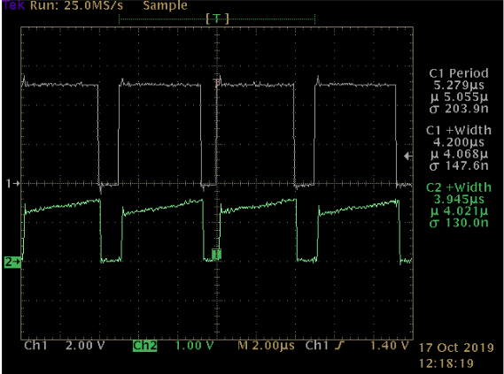
  • Switching speed:  200kHz
  • Cooling: natural convection
  • Operating temperature: -20 - +50C (not validated)
  • Bias current:  53mA running, 26mA idle
  • Efficiency >95% (@ 90%+ loads)

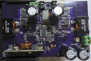
This design is based on the 12 to 5V USB charger and uses the same PCB, PIC, and switching core.  PCB modifications have been made with hand wire traces, trace cuts, and glued components.

The switching core of the charger remains a non-isolated synchronous buck with limited low-side control.  Unlike 125vbuck, Current mode control with slope compensation is employed.  A type 2 error amp in the outer control loop 
regulates the charger voltage.

An RS232 interface shared with the ICSP circuit provides a console interface with a robust command set to allow experimentation without firmware modification.  Many parameters are stored in Non-Volatile Memory (NVM).

    RS232 settings: 115.2kbps, 8 data bits, 1 stop, no parity

This console port is accessed over the micro-USB connector on the PCB and is optimized for use with a GBIB-style control program.  A query command is also provided to support the rs232-44780 display unit.  This command responds with a packet of binary data that is rendered on a Hitachi 44780 style LCD indicating unit status, battery, and PV output.

The console / display interface is optional and the unit will operate without it provided that the proper options are set (e.g. closed loop and autostart).

A status LED on the PCB indicates if the charger is running (Green) or in a stopped or fault state (RED).  There are no flash sequences used to communicate a status code.  The LED is managed by the Initialization and Charger on/off functions.

mpptproto-1_1-b20.zip

Source code: replaces low output voltage check with over-current & addition of 'sweep' P&O algorithm.

Zip Archive - 45.21 kB - 02/16/2020 at 13:13

Download

binary.h

Shared include file required to build the firmware.

x-chdr - 883.00 bytes - 11/01/2019 at 01:19

Download

mpptproto-l1-r1.pdf

Design spec sheet for buck inductor.

Adobe Portable Document Format - 67.85 kB - 10/31/2019 at 18:03

Preview
Download

mpptproto-config-191030.pdf

PDF of PIC peripheral configuration for gate drive, control loops and synchronous low-side.

Adobe Portable Document Format - 21.70 kB - 10/31/2019 at 18:02

Preview
Download

mpptproto-config-190613.sch

Autodesk Eagle schematic as-built. Only install components from BOM that are also listed here. Additional components have part# attribute with Digikey part number.

sch - 31.93 kB - 10/31/2019 at 18:00

Download

View all 10 files

  • Post-Mortem #2

    Brian Cornell02/16/2020 at 13:11 0 comments

    Replace bad code with more bad code.  I should know not to post before testing but not much time to get things done right now.  It turns out that moving the low output voltage code to the main run loop just made things worse.  Low voltage conditions are a regular occurrence during the MPP scan.  So I got rid of that diagnostic entirely.  It was there mainly as a HW safety check and as this shows it doesn't contribute.

    In its place I added a check for over-current.  Originally I opted to skip this since I didn't intend to conscript this into any kind of regular service - and it uses current mode control which is built-in protection.  But when the PV panel has high potential a short in the switching core or output might create a hazard.

    Yesterday's code has been updated.

  • Postmortem Updates

    Brian Cornell02/15/2020 at 21:18 0 comments

    For anyone that really wants to build this thing I've posted updated code containing two improvements.  Firstly, I fixed an annoying firmware failure mode that would require rebooting the charger when clearing snow off the PV panel.  It wasn't a bug - just bad code.  During the charger start sequence I had a check for the charger's output voltage less than the battery - a simple way to tell if there was a HW problem.  But I did this without checking the PV voltage first.  Fixed by moving the check into the runtime loop where a true low PV volts condition would trap first.

    Second, I wasn't satisfied with heuristic P&O algorithm.  It spent too much time bobbing about the MPP mean and wasting energy.  I worked on improvements but it got more complicated than I wanted.  Instead I came up with the 'sweep' algorithm which made it much simpler to find & lock on the MPP.  Not perfect but much better than the heuristic version.

    All updates are documented in-line and you can select which MPPT algorithm to use with a compile constant.

  • Design Challenges

    Brian Cornell10/31/2019 at 20:44 0 comments

    A non-isolated buck is simple and that enhances durability and efficiency.  But the details of how it is implemented can present challenges.  For this project there are three:

    1. Output relay (SSR) and non-isolation between PV & battery
    2. Low-side synchronous control
    3. Current sensing

    Output Relay.  The problem with any design that must deal with external voltages present on both its input and output is preventing current reversal - e.g. the flow of current from output to input.  In isolated designs this is generally not a problem.  In non-isolated designs the easy solution is a blocking diode; but these introduce losses.  In this design, 100W at 14V is 7.14A.  The best schottky might get close to a Vf of 400mV but that is still (7.14 * 0.4) = 2.85W.  Paralleling doesn't help, it just distributes the loss over more components.

    An SSR (Solid State Relay) solves the efficiency problem.  The custom design in this unit has an on resistance ~ 5.3mΩ, so the loss from the above example would be (7.14^2 * 0.0053) = 270mW.  The problem with an SSR is that it cannot be left on when the buck is not running:  battery voltage would forward bias the high-side MOSFET body diode.  A secondary problem could be turning the buck into a boost (again, in reverse) depending on how long the low-side MOSFET is turned on: too long and the inductor will charge and attempt to discharge its energy when the low-side is turned off.

    The design avoids these deficiencies thru firmware control and leveraging the best of both worlds.  At low loads the SSR is kept off and output current flows thru the SSR's body diode.  At higher loads the SSR is on.  Since there's no output current sense, PV current is used as a proxy.

    Low side control.  Low side synchronous control is best done in hardware by sensing the flyback current.  This design doesn't accommodate, so on-time must be estimated based on operating conditions.  Like the output relay, the goal is to minimize losses by having the majority of current flow thru the MOSFET and not its body diode.  I derived a few approaches to this problem in my Synchronous Buck Control project.

    A somewhat simpler, binary approach is used here.  At light loads (based on PV current) a minimal on-time is maintained (few hundreds nS) that is enough to maintain bootstrap capacitor charge but not long enough for current reversal.  At higher loads, approximately when the inductor is expected to be in continuous conduction, the on-time is increased to a value slightly higher than the longest on-time possible under any load conditions.  In effect, it removes the restriction from the hardware control loop and allows it to determine on-time based on duty cycle.

    Current sensing.  Actually, this isn't a challenge for the current design but possibly one for future, higher power designs.  The unidirectional current transformer is a super-clean and simple method to sense current in a switching supply.  Here's a 'raw' sample taken from the prototype running close to max load.  The probe is a passive Tek P6563A 20x (9.5MΩ impedance, 4.5pF):

    This was probed at the MCU's pin.  There is no conditioning circuit; just a buffer resistor between the sense circuit's output and the MCU.

    This has a big impact on the current mode control method.  To ensure loop stability and minimize jitter the S/N ratio of the current signal seen by the comparator (comparing to the slope compensation ramp) must be good.  Other methods usually involve some type of shunt resistor and will require active conditioning to remove the noise without distorting the signal.  This is why most modern current mode supplies employ a monolithic control chip with all of that stuff built in.

    The problem with unidirectional current transformers is that the core must be reset on each cycle and that requires time.  Running at 200kHz, as this design does,...

    Read more »

  • MPPT Algorithm

    Brian Cornell10/31/2019 at 19:29 0 comments

    Any power supply connected to a source impedance that is variable and often higher than its own must modify its operation to match impedances as closely as possible for maximum efficiency.  This design uses duty cycle for impedance matching and works as follows (refer to the peripheral config schematic for details).

    The hardware control loop, consisting of an inner peak current and outer voltage loops, runs without interference from the firmware.  The comparator output from that loop drives a falling event to the COG that sets duty cycle.  The maximum duty cycle of the unit is governed by the master PWM and also generates a falling event to the COG.  The COG works on a first come, first serve, basis:  the first falling event ends the DC (subsequent events are ignored).  Under normal circumstances (without MPPT & low source impedance), the HW control loop would always generate the falling event.

    The MPPT firmware manipulates the maximum allowable DC by modifying the master PWM's DC.  When the PV output is low (high impedance), it will set a low maximum DC.  Regardless of what the HW control loop demands the master PWM will terminate the DC first.  During periods of high PV production (low impedance) and/or loads less than 
    available energy, the master PWM DC will be set high and the HW control loop will terminate the DC.  Of course the side effect of this scheme (or any that manipulates the power supply's impedance) is that the output voltage will often be less than what the HW control loop demands.

    The algorithm consists of two sections.  The first moves the duty cycle a fixed increment, defined by S_TM_MPPT_DC, in the direction indicated by the bit flag mpptIncrease when the bit flag mpptMove is set TRUE.  Evaluation of the results of moving the DC is handled by the second section.

    When the DC is moved there is a mandatory delay defined by constant 
    S_LM_MPPT_COUNT which specifies the number of RUN loop iterations that must complete.  This is done to reduce jitter and 'hunting'.  Because it uses loop iterations and not a fixed timing source it's important to know the average loop execution time since this forms a primitive filter.  This can be measured by uncommenting the constant
    _TIMING_RUN in mpptproto.h and probing one of the LED pins.

    When the timer expires the current PV power is compared to the MPPT's previously sampled power.  If less the DC direction is reversed since it's assumed that the peak was passed.  If equal, no change is made and a new delay/sample taken.  This method creates a sweeping motion over the available PV power range.

    Even in static conditions the algorithm hunts.  Adding hysteresis (similar to the fault monitoring method) would likely help.

  • Description of Operation

    Brian Cornell10/31/2019 at 19:23 0 comments

    What follows is a summary of how the unit operates.  For details review the firmware: it is thoroughly documented.

    The unit is based on a Microchip PIC16F1769 8-bit, mid-range CPU with peripheral support optimized for SMPS applications.  It has two functional blocks: 1) a hardware-based synchronous buck, and 2) a firmware-based Maximum Power Point Tracking (MPPT) control loop.  The firmware also monitors system parameters, manages operating modes, and provides a simple GPIB-style console interface.  Many of the unit's operating parameters are store in Non-Volatile Memory (NVM - program high-endurance flash) and can be modified via the console.

    The unit is powered by the 12V battery it is connected to.  This was done to avoid the added power conditioning & regulation circuitry that would be required if the PV was used.

    The PIC's 10-bit Analog to Digital Converter (ADC) is used to collect the necessary data points:

    • PV voltage & current
    • Battery voltage
    • Output voltage

    PV power is directly calculated from the individual PV values.  There are a few drawbacks to this.  First, the ADC can only do one conversion at a time so PV volts & amps are obtained sequentially.  Second, while it is DC, there could be significant amounts of ripple depending on load, available sunshine, etc,.  This design doesn't have the capability to perform an RMS calculation.  To compensate, a fair amount of bulk capacitance exists in front of the buck and the PV values are averaged over several samples.  Observationally, these deficiencies do not appear to have a material impact.

    Refer to the peripheral config schematic for details.

    The synchronous buck employs the peak-mode current control method to achieve regulation.  In practice, this consists of two layers: the inner current, and outer voltage control loop.  Slope compensation is used to eliminate sub-harmonic oscillation.  Low-side control is managed in a hardware control loop.  On-time is set with a voltage reference that is controlled by firmware.

    The Perturb and Observe (P&O) method is used to achieve MPPT and is executed in firmware.  The algorithm monitors PV power and works to match the unit's impedance to the PV's by limiting the maximum duty cycle (DC) of the buck.  Basically it looks for peak PV power.

    Firmware also manages the operating mode of the unit.  During low light levels it shuts the buck down and enters a low power state to minimize battery drain.  Charging automatically resumes when the PV voltage is sufficient.  Detected faults will halt operation if an unrecoverable error is detected

  • If You Build It

    Brian Cornell10/31/2019 at 18:36 0 comments

    If you really want to build this as documented you'll need to go thru some hoops.  Keep in mind that it is a prototype and doesn't contain the refinements and circuit protection features of a finished design.

    1. Go to the 125vbuck project to get the clean PCB and have it manufactured.  But if you're willing to go thru that effort I'd suggest that you modify the board following the mods in this project to make assembly much easier & cleaner.  Otherwise you will need to hack your shiny new board according to the board PDF in this project.
    2. Reconcile the BOM.  The design workbook has the BOM from 125vbuck project.  Reconcile with the schematic and only install what the schematic lists.  There are additional parts on the schematic, specific to this design.  Most of those contain a Digikey part number; a few don't and their specs / tolerances aren't critical.
    3. Wind the inductors.  The design workbook should provide what's needed (core #s, wire gauge, # turns, etc.) for the buck & current transformer.  The core part # for the SSR flyback is in the BOM.  The primary is 6 turns and the secondary is 17.  Use 28 AWG magnet wire.  Be sure the polarities are opposite one another when installed; it should output ~ 12-17V across the MOSFET G-S.
    4. Consider adding fuses, particularly on the battery side.
    5. Connect to the battery first (then the PV).  Otherwise it's possible that the PIC will be damaged (pin protection diodes will forward bias since Vdd isn't applied).  A short could also develop between the high & low side MOSFETs since the gate driver isn't energized: the gates might float and turn on.
    6. Exercise care when working on an energized unit.  While the working voltages are less than 30V, the reset voltage on the current transformer can reach 100V at high loads.  Be careful when probing.

View all 6 project logs

Enjoy this project?

Share

Discussions

Similar Projects

Does this project spark your interest?

Become a member to follow this project and never miss any updates