This is the next iteration of my solar charger work. The last one, Solar Charger & Balancer, was intended to handle a string of PV panels in a mix of parallel & series configurations, and included a battery balancer. PVC follows the trend with residential inverters and is designed as a panel level charger that can handle up to 500W and dumps a regulated 56V onto a common rail that can be aggregated with other panels to charge a battery stack. It also incorporates the hardware MPP tracking design that was proved out in Solar Charger & Balancer.
I chose to stick with 56V because it is a relatively safe voltage and doesn't require insane currents to get to a few kilowatts. Sticking to moderate voltages also reduces design complexity, component stresses, and cost. Whereas Solar Charger & Balancer used a SEPIC converter, PVC is a dirt-simple, non-synchronous, non-isolated, flyback. There's no requirement to buck & boost the panel voltage since even the most efficient 500W monocyrstaline panels' MPP voltages are well below 56V. It is significantly smaller because of this.
PVC is intended to bolt directly to the back of the panel and connect to a common bus that charges the battery. With independent converters, some sort of controller is required to coordinate the chargers and protect the battery stack from being over charged. It is possible to include a charge algorithm in PVC's firmware, but it would be nice to have some centralized control to monitor the total charge in & out, health of the panels/chargers, etc. So, I have decided to use Power Line Communication (PLC) to communicate with the chargers. The PLC & controller will be added to the next design revision: this initial design only includes the converter core.
SPECS
Preliminary specifications of development board based on bench and limited field testing. With a Vin less than ~ 32V, the output power will be thermally limited. In reality, most PV panels with MPPs less than 35V are rated for 400W or less and will be the limiting factor.
- Vin: 25 - 40V DC
- Ain: 13.3 - 21.3A
- Vout: 56V
- Aout: 8.9A
- Pout: 500W
- Peak efficiency: 95.7%
- Average efficiency: 94%
- Topology: interleaved, non-isolated & non-synchronous flyback
- Switching frequency: 200kHz
- Control mode: peak current
- Controller: PIC16F1776
- MPP method: hardware tracking of Vin
- Cooling: natural convection via heatskink to case
- Operating temperature: -40 - +50C unverified
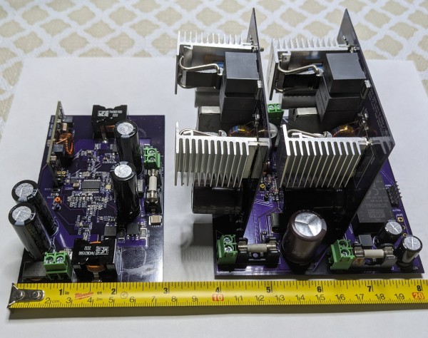
- PCB dimensions (LxWxH): 11.5x7.2x4cm (4.53x2.83x1.57")
THEORY OF OPERATION
The converter consists of two non-isolated flybacks running 180 degrees out of phase. This reduces peak currents in the plant and reduces input/output current & voltage ripple. Each phase employs an inner current mode control loop that manages the duty cycle with an outer common voltage loop. In theory, this ensures that the power output of both phases is equal. A low-side MOSFET and Schottky output diode form the plant switching pair, and each contain an RC snubber to control ringing.
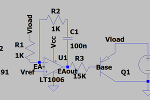
Input & output voltage sensing is performed with resistive dividers that provides the sense signal for both the input & output voltage control loops. Current sensing is performed with a high-side sense resistor and an amplifier that provides the appropriate ramp signal for the current loop. Since the amplifier's bias positive supply is Vin, a level shifter (Q101, Q103) is required to ground reference the signal. R101/R108 & R113/R117 set the gain for each phase.
The Microchip PIC controller configures peripherals (Opamp, Comparators, timers COG, PWM, PRG) at boot so that the converters operate autonomously. With the exception of output over-volt protection, the PIC MCU functions as an administrative controller that provides an RS232 console interface and manages the startup configuration. Various operating parameters are stored in NVM including MPP tracking voltage, output voltage, current limit, etc.
A type 2 compensation network is used for the output voltage control loop: the error signal...
Read more »
Hi Dan, yes. The revised PCB will include a mounting bracket that doubles as a heat sink to conduct heat from the board to the case.