2022/10/13 : The badge is officially unveiled !
Have a look at the definitive project page :
#BADGE FOR 2020+₮ SUPERCON (₮=years of lockdown)
and the announcement at https://hackaday.com/2022/10/12/the-2022-supercon-badge-is-a-handheld-trip-through-computing-history/
The rest has not been touched in more than 2 years now... It is only preliminary.
I called this project "v0j4" because
- "Hackaday Belgrade Conference 2020 badge CPU" doesn't particularly roll on the tongue
- It's a 4-bits CPU so it needs a 4 in its name
- It's designed by @Voja Antonic
- Voja's name ends with a "A" and it looks like 4
- It looks g33|<y and I replaced a o with 0 for extra ha><0r credz.
- It's short, cute and unencumbered
- It's too late now to change it, muhahahaha.
Short description of the architecture
- The datapath is 4-bits wide (it's nibble-oriented)
- Harvard, load/store RISC-y minimalised architecture (with much inspiration from the PIC family, it seems)
- Instruction words and instruction addresses are 12 bits wide
- Instruction memory is 4096 words
- Data memory is 256 nibbles (128 bytes), that can be accessed with immediate or register operand for load and store
- Register set mapped to data memory page #0 (addresses 0-15) so it can be displayed.
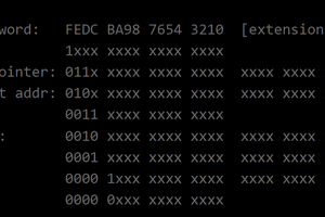
- 8 levels of stack (mapped to data memory page #1 at 0x10+3×[SP] )
- 4 bits of output and 4 bits of input GPIO, register-mapped, accessible on the external connector of the badge
- 2 condition flags : Z and C
- Conditional execution : skip from 1 to 4 instructions forward
- Relative Jump : -128...+127 instructions
All instructions fit in 1 word and execute (more or less) in 1 cycle.
- 15 instructions (left side of the board) use a 4-bits opcode with two 4-bits operands (register name or immediate) or a 8-bit immediate value
- 16 instructions (right side of the board) use a 8-bits opcode (with 0000 in the MSB) with 4 bits of operand and/or condition
- RET might need 3 cycles (3 reads from RAM) to fetch the return address.
There are 16 registers :
- R0 to R9 are GPR
R0 can be the only implicit operand of OR/AND/XOR/ADD/CP/RET with immediate,
R0-R3 can be used by the bit set/clear/test/toggle opcodes - IN : read the 4 input bits of the GPIO connector
- OUT : writes to the 4 output bits of the GPIO connector
- JSR/PCL/PCM/PCH : destination address for jump/call
There is no JMP or CALL instruction. Instead :
- load PCL/PCM with immediate 8 bits with LPC opcode
- if you want to jump, write the destination to PCL
- if you want to call, write the destination to JSR
- RET modifies R0 with an immediate value (useful for lookup tables)
More fun stuff :
- The board has room for 15 programs, each 4096 instructions. Program #16 is read from the outside (serial port ?)
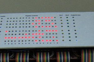
- There is a 16×8 LED raster screen that displays 2 adjacent banks, selected by the DISPAG #N instruction. By default, it displays banks 0 and 1, the register set and the stack, to show how a program evolves.
- One serial port is available (how is it accessed ?)
- There's a SAO port ! (needs to be documented too)
- Program memory has some config words at the end of the space to configure serial port, registers where handshaking is located, the pressed buttons, a short serial receive buffer...
- There is some crude support for real time synchronisation with rolling values updated in RAM (tbd).
The badge implements the v0j4 with a PIC24 while explicitly detailing internal circuits on the silkscreen.
- Will somebody implement it with a FPGA ? Discrete transistors ? TTL/CMOS circuits ?
- The PIC24 emulates v0j4 at about 100-150K ips. What about a Python emulator ? JavaScript ? What is reasonably possible at that level of performance ?
- What about extension I/O boards ? Alpha LCD ? Buttons/keyboard ? Bluetooth I/O ? 8255 ? relays ? SPI ? I2C ? external serial Flash memory ? PS2 mouse & keyboard ? Speaker/beeper ?
- What about the applications ? Games (Snake, Tetris, Conway's Life...) ? Utilities (scientific calculator, PLC) ? Libraries (BCD computation library, LCD,...
 Yann Guidon / YGDES


 Pavel
Pavel

 Erik Piehl
It's not "more or less" in 1 cycle, all instructions really execute in 1 cycle (well, mostly with a 1-nibble data field, but there's always the limitation with every processor). If you have prepared high and med nibble for long jump/call, you need only one instruction (write to PCL or JSR register) to JMP or CALL subroutine.
For instance, to read data from lookup tables (table contains "return #N" instructions):
- You preset PCH and PCM registers
- Write to JSR, which is call sub (computed calls are possible)
- on return, R0 contains the table data
- write or use somehow the data
- increment JSR (this will cause new CALL addressed to the next nibble of data
- and then only INC JSR, INC JSR... every time you have the new data in R0
Note: INC/DEC JSR/PCL are 12-bit instructions, carry-propagated to registers PCM and PCH, and executed as CALL or JMP.