David H Haffner Sr
-
Problems Have Caused A Major Re-Design
01/17/2017 at 20:25 • 4 commentsOK, the first problem has occurred with using the DVD piece as my diffraction grating, even at 4.7G and 1540 lines per mm, and the DVD begin a name brand, doesn't mean a thing. There is no way around the random spacing errors created by the manufacturing process for a ruled grating type piece.
I thought by using the Schott glass filter (which is designed to reduce these effects at the detector,) would help, but it does not. Alignment is another problem, even though I have it designed so I can rotate it, it doesn't matter, the lines MUST be parallel, with little spacing error.
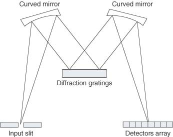
So I am going to have to use a Holographic diffraction grating square. the specs will be in the component list. I am going to use the Czerny-Turner configuration which is shown below:
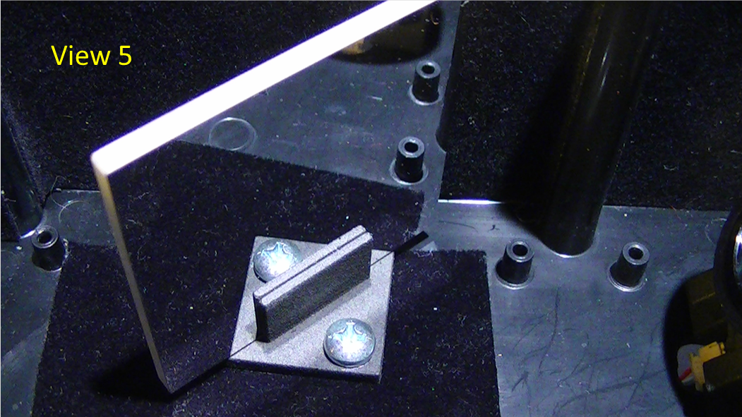
I am still using the flat silver coated protected mirrors because of their superior reflectance. I will just have to add a second mirror as shown above.![]()
This set up will just solve a lot of headache, especially since I have designed my own fiber optic mounts (FC/FC connectors.) I am still able to use my present set up for testing the fiber optic equipment I've built.
All this will still fit nicely within the enclosure with room to spare, so no worries there, just a slight rearrangement of components.
-
Addendum To Log # 44
01/14/2017 at 12:45 • 0 commentsFrom the specifications sheet for the JDEPC-05 cmos sensor;
![]()
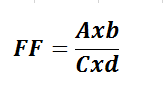
To find a theoretical MTF curve for a sensor, it is necessary to know three characteristics of the sensor: the active sensing area, the area comprising the sensing area and the interconnection and support structures ("real estate"), and the total number of those areas (the pixel count). The total pixel count is almost always given. Sometimes the overall sensor dimensions are given, from which the real estate area can be calculated. Whether the real estate area is given or derived, if the active pixel area is not given, it may be derived from the real estate area and the fill factor, where fill factor is the ratio of the active area to the dedicated real estate area;
![]() Where
Where- the active area of the pixel has dimensions a×b
- the pixel real estate has dimensions c×d
So in the case of the JDEPC-05 cmos sensor, our effective pixel area is; 3590 * 2710 um, this is our pixel “real estate,” our active area is 2.2um * 2.2um![]()
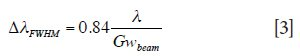
= 0.49 X 100= 49 % theoretical MTF from the table below, this is for a CCD detector but the resolution principle is the same. Row # 3 shows a horizontal pixel resolution of 1024 pixels and its corresponding resolution at the appropriate wavelength. Our wavelength is 532nm, so I will just recalculate this equation to fit my wavelength;![]()
0.84 x 532/1540 x 4.8 = 1.39nm pixel resolution![]()
Process Raman typically requires ~10 cm-1 resolution, so with a 1024-pixel detector (4.5 cm-1/pixel sampling as seen from Table I) we should be able to obtain the required resolution.
*a quick note, the values in the table above refer to horizontal pixels, so in closing, the JDEPC-05 cmos sensor has 4.8 cm-1/1.39nm resolution @ 532nm, more than adequate for detecting Raman signals. - I also want to close with this thought, I have a poster of Einstein that I have had since I was in high school, and it is a quote of his; “The definition of genius is taking the complex and making it simple.”
-
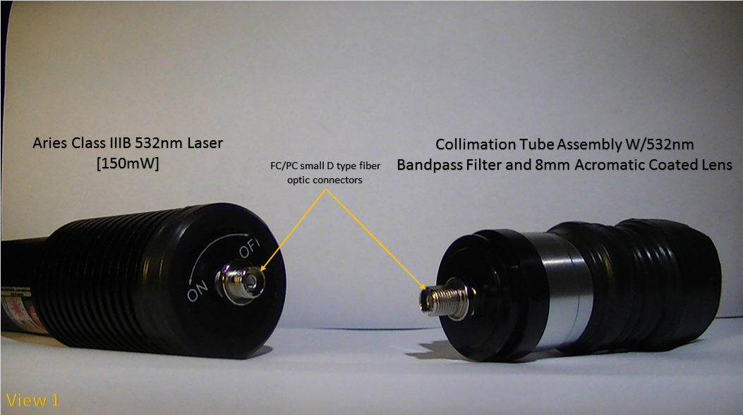
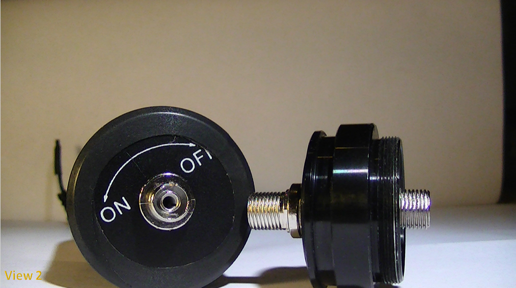
Fiber Optic FC/PC Connectors Completed
01/13/2017 at 10:04 • 0 comments![]()
![]()
![]()
![]()
Holes for the Laser head were tapped with an M8 x 0.7mm tap and an M8 x 1.25mm tap. The collimation tube head was tapped using the same method. On the collimation tube assembly, the tapped head is an 6mm telescope eye piece with the lenses removed, so I just drilled the hole out about 1mm wider in diameter and taped it out to 8mm to fit the connector.
You may notice on the collimation head picture that, there is a double FC/PC connector on both sides, this is accomplished simply using the shorter ends of the connectors and screwing them in end to end. I didn't have to do this, but I wanted the beam as close to the lens as possible to reduce any chance of internal reflections.
-
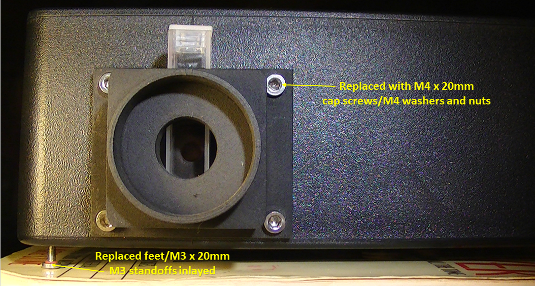
Fixed and Replaced Cuvete Holder Screws and Feet
01/12/2017 at 13:17 • 0 commentsFinally, my M4 hardware kit from ThorLabs came in and I was able to fix the cuvette holder and also make the feet adjustable, using the M3 brass standoffs inlayed on the bottom and the M3 's screw right on in.
![]()
The kit item # is; HW-KIT1/M
-
Bill Of Materials
01/11/2017 at 12:47 • 0 commentsHere is the current bill of materials for this project, I had to readjust the project goal parameters from under 700.00 dollars US to under 1000.00 dollars US, it just couldn't be helped.
![]()
-
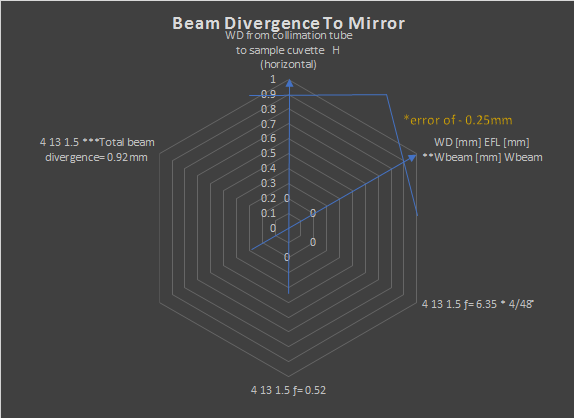
Data Results For Laser Collimation Tube Assembly Log#44
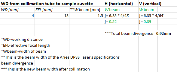
01/09/2017 at 18:42 • 0 commentsWell, here it is, the data, at least for the laser collimation tube. I imaged the laser's factory specification beam divergence (beam width) against the divergence of the laser tube and the data is clear, I now have a Wbeam divergence of 1.6mm which with the new calculations of; F= 6.35mm * 4mm/48 deg = 0.52mm horizontal FOV.
Which also translates to a 58 percent decrease in beam width (which is exactly what I was aiming for.) Now I have a beam width of 0.52mm. A word of caution though, all these calculations are approx. values, even with the math, although the optical lenses I used, have specs attached to them, there is still an error rate of about -0.25mm plus or minus.
*The 0.92mm total beam divergence is the total of horizontal and vertical pixel sums.
![]()
Below are the calculations associated with this plot;
![]()
![]()
Below are the calculations associated with this plot;
![]()
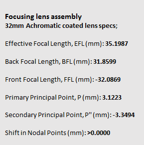
Here are the specifications for the 32mm focal lens to mirror assembly;
![]()
![]()
![]()
-
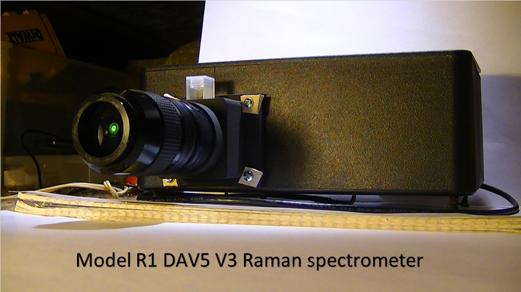
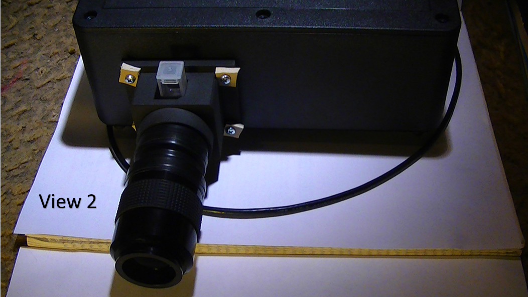
*UPDATE* Model R1 DAV5 V3 Raman Spectrometer
01/07/2017 at 16:44 • 0 commentsAll the new re-designed parts are installed and tested, data coming soon...
![]()
![]()
![]()
![]()
![]()
![]()
![]()
![]()
-
Mathematical Details for the DAV5 V3 Raman spectrometer/Cmos sensor focal equations
01/05/2017 at 16:10 • 0 commentsMathematically speaking, the idea behind this design was based on a DIY Raman spectrometer I ran across a year ago, its simplicity caught my attention and after studying their research results, I was convinced I could build one using a cmos sensor based design since these cmos sensors operate quite well in the green wavelength range of the spectrum.
The JDEPC-05 turned out to be a surprising little detector, one, because it had a great spec sheet with a lot of detail and because of this, I was able over time and much trial and error, to come up with my present design concept.
One critical factor with this sensor, is removing the IR window underneath the lens, it does introduce a small amount of extra noise but expands the dynamic range when readjusting focal length calculations. Keep in mind though that a cmos has a wavelength limit of 1100nm, which is fine for this design using a 532nm green laser source.
Now, with much research and using these equations, I have successfully aligned and focused the sensor to mirror ratio in relation to the relative horizontal and vertical spectral image striking the actual sensor substrate.
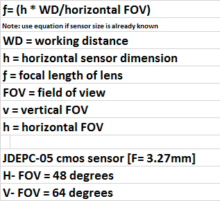
The factory specifications for the JDEPC-05 has a focal length of 3.27mm @ 48 degrees. Since I am using a 32mm achromatic coated lens, (to capture more incoming light,) coming from the exit slit, I had to not only adjust the focal beam width of the image to the mirror but the one going to the sensor, since the actual sensor size is 6.34mm (0.25’’.)
Here is the math;
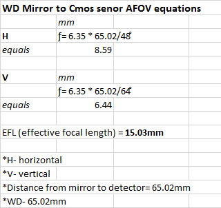
![]() Focal distance from apex of 32mm lens to mirror is; 70mm. From centerline of mirror to sensor is; 65.02mm.
Focal distance from apex of 32mm lens to mirror is; 70mm. From centerline of mirror to sensor is; 65.02mm.F= (6.34mm X 65.02mm/48 degrees)
H= 8.5mm (0.33’’) focal distance from mirror to sensor
F= (6.34mm X 65.02mm/64 degrees)
V= 6.43mm (0.25’’) focal distance from mirror to sensor
![]()
Entrance slit width= 6.34mm
Exit slit width= 100um
Laser beam width= 0.37nm (as of present.)
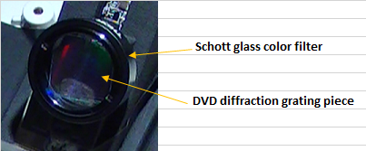
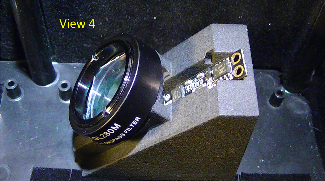
Distance from apex of sensor lens to DVD diffraction grating is 3mm (this may have to be adjusted slightly by hand, using a CFL spectrum as your focal guide. You need to image the CFL spectrum in “live capture” mode so you can see the lines come into focus…yes, it is very difficult but I have no other way of resolving this procedure.)
There is no need to use a very expensive holographic or other diffractive piece other than the DVD piece, if you adjust the alignment correctly. I will outline this procedure next;
![]()
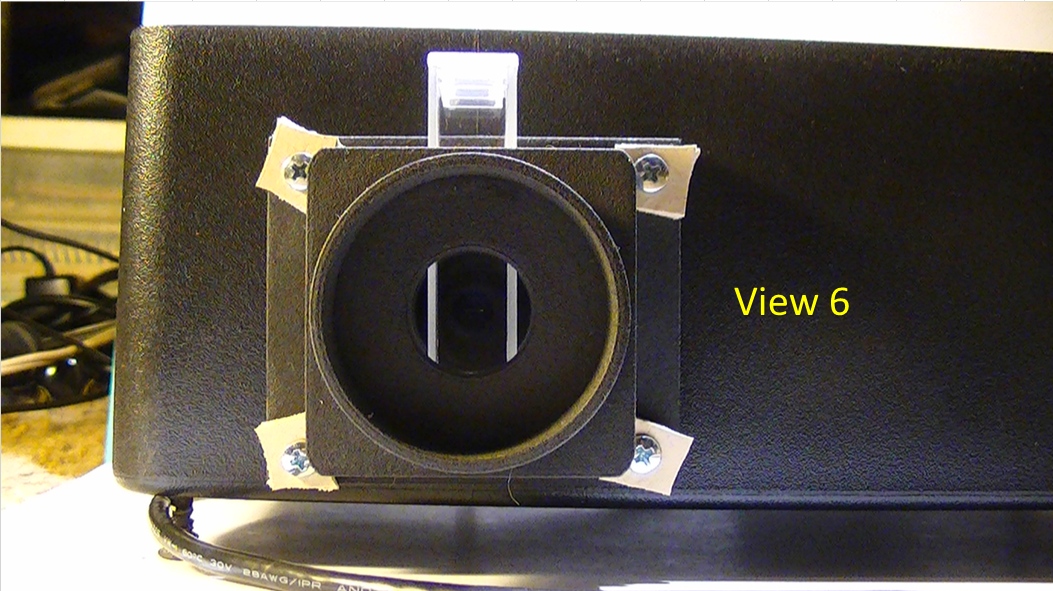
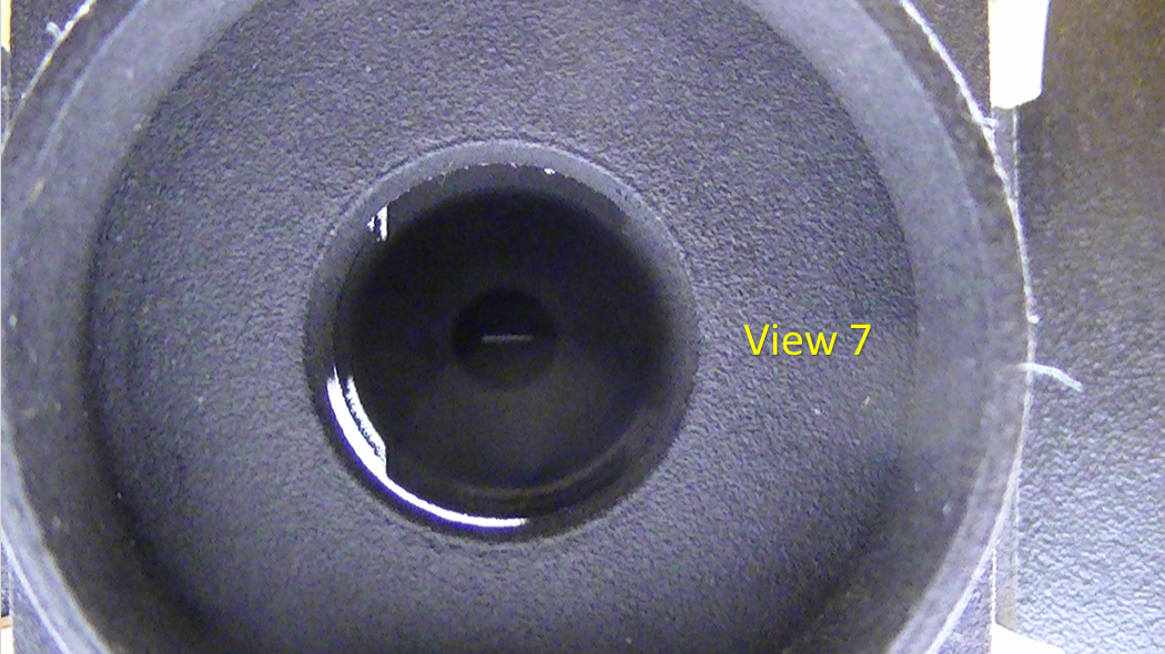
In the figure above, you see the DVD piece secured in the filter housing by a locking sleeve, the entire filter housing fits on top of the cmos camera mount, and can be rotated in either direction. This feature allows not only DVD diffractive alignment, but provides an accessible method for removing the diffraction grating for replacement.
This is where the distance is measured from the bottom of the filter glass to the apex of the cmos lens (3mm approx.) In this way, you can easily utilize an inexpensive DVD R/W CD to use as your diffraction grating and it will work just fine.
This one is a 4.7G 1540 lines per mm piece. I have used the 8.5G pieces before and the resolution is a little sharper, but you will sacrifice your wavelength range by doing so, and in this case, this diffractive value is working great.
So, alignment is quite easy, just turn in either direction very slightly until you have the lines as vertical on the screen as possible. Now, depending on the processing software you are using you do need to see the spectrum in real time, to align it correctly.
You will know it is aligned correctly by watching the green (546nm peak) you should have at least two sharp peaks with NO clipping, if you get clipping just attenuate the signal slightly with an NG filter, (doing this though, keep in mind may change the wavelength values at the peaks and change their shape, try to find the best balance and keep it there.)
In my next log, I will explain the theory of operation behind my laser collimation tube design.
-
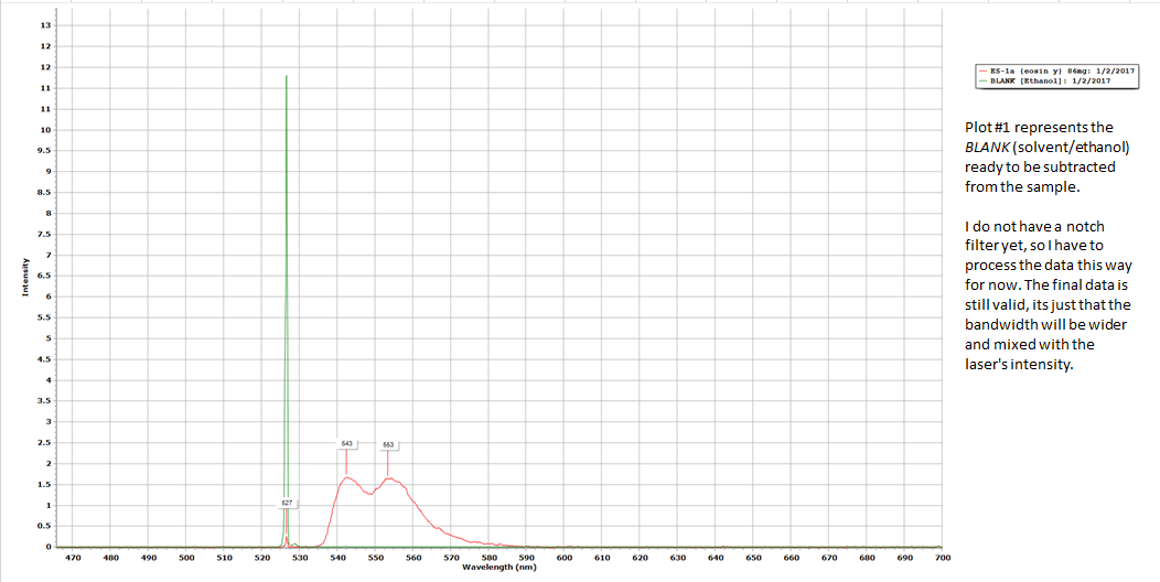
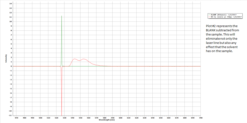
Absorption/Emission Spectra Of Rhodamine B In Ethanol
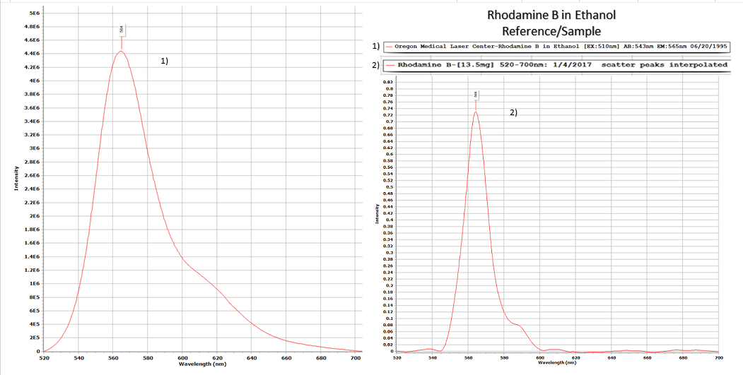
01/05/2017 at 11:59 • 0 commentsLog#41; Further qualifying the UV/VIS functionality of the DAV5 V3 Raman spectrometer by imaging a sample of Rhodamine B (Rhodamine dyes are used extensively in biotechnology applications such as fluorescence microscopy, flow cytometry, fluorescence correlation spectroscopy and ELISA.)
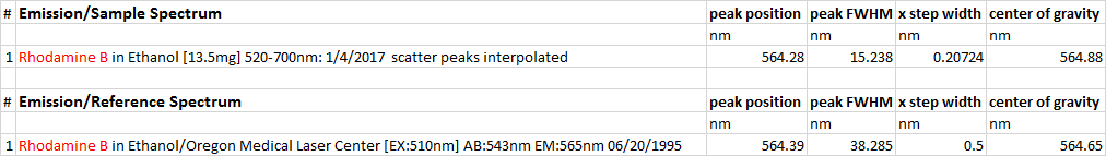
In fig.1, To the left is my reference spectra (Rhodamine B in Ethanol from the Oregon Medical Laser Center/Using a SpexFluoroMaxII Fluorometer) To the right, is my sample of Rhodamine B in Ethanol using my DAV5 V3 Raman spectrometer.![]()
The reason the FWHM values are different between the two spectra are, because the SpexFluoroMax II, uses a Xenon lamp as the broadband light source and a CCD detector. The DAV5 V3 uses a JDEPC-05 cmos 0.25'' board level detector and a 532nm DPSS laser source.![]()
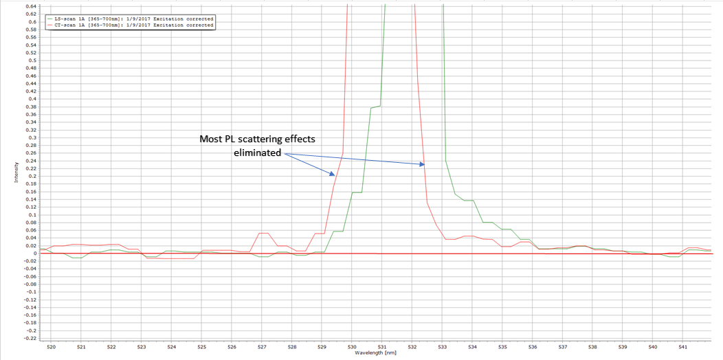
Note that this does NOT in any way diminish the data, as you can see that the spectral shapes are nearly identical.
In Fig.2 above, this is an absorption and emission spectra taken with the DAV5 V3 spectrometer. The absorption spectra was obtained using a Solux lamp/50W/12vdc/5A/4700K. The emission spectra was obtained using an Aries 532nm DPSS green laser/150mW/3vdc.![]()
![]()
Samples were prepared in 1cm pathlength quartz cells with absorbance less than 0.1 at the excitation and all emission wavelengths to uniformly illuminate across the sample, and to avoid the inner-filter effect. The dark counts were subtracted and the spectra were corrected for wavelength-dependent instrument sensitivity.
References:
http://omlc.org/spectra/PhotochemCAD/html/009.html - rhodamine b in ethanol
http://www.turnerdesigns.com/t2/doc/appnotes/998-5111.pdf - tracer dye prep
-
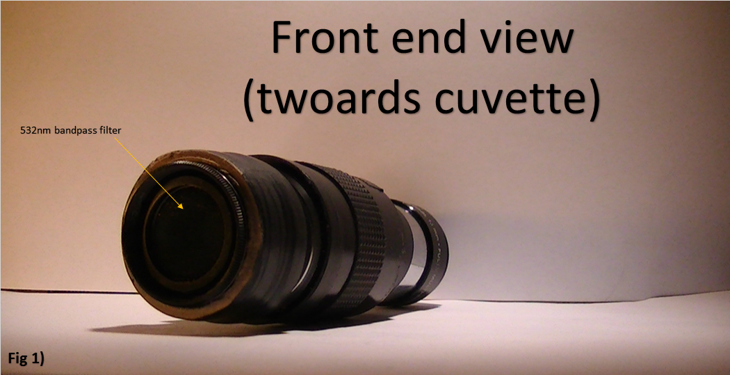
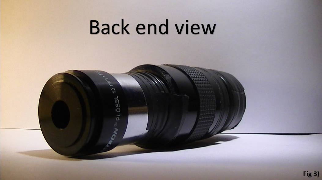
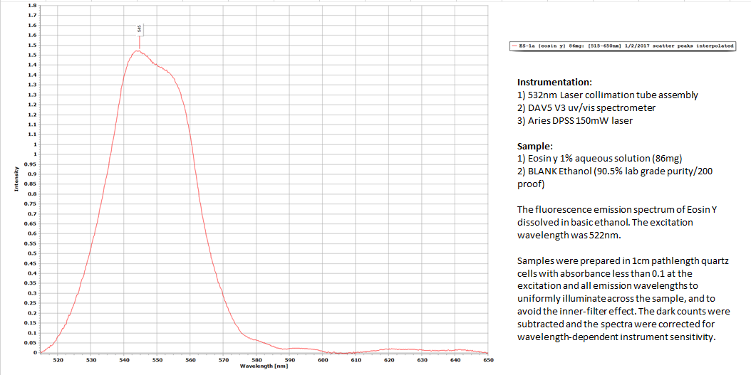
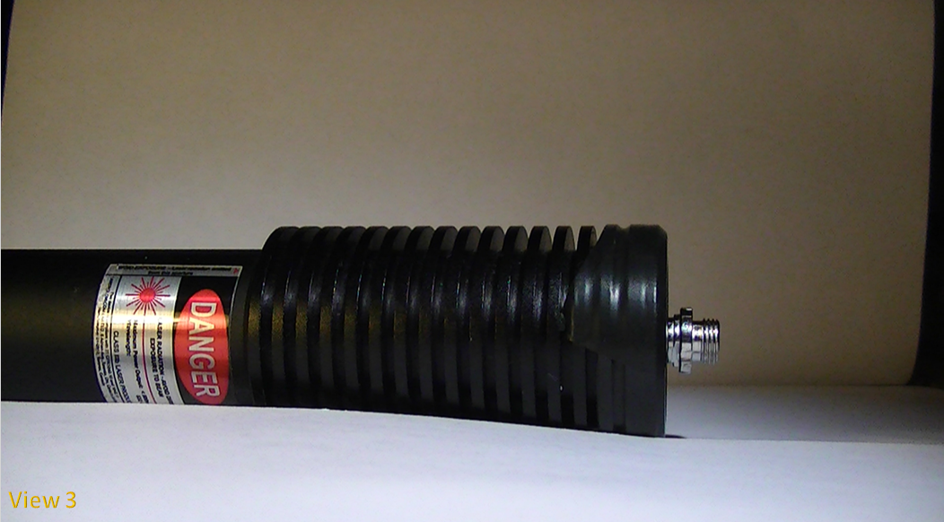
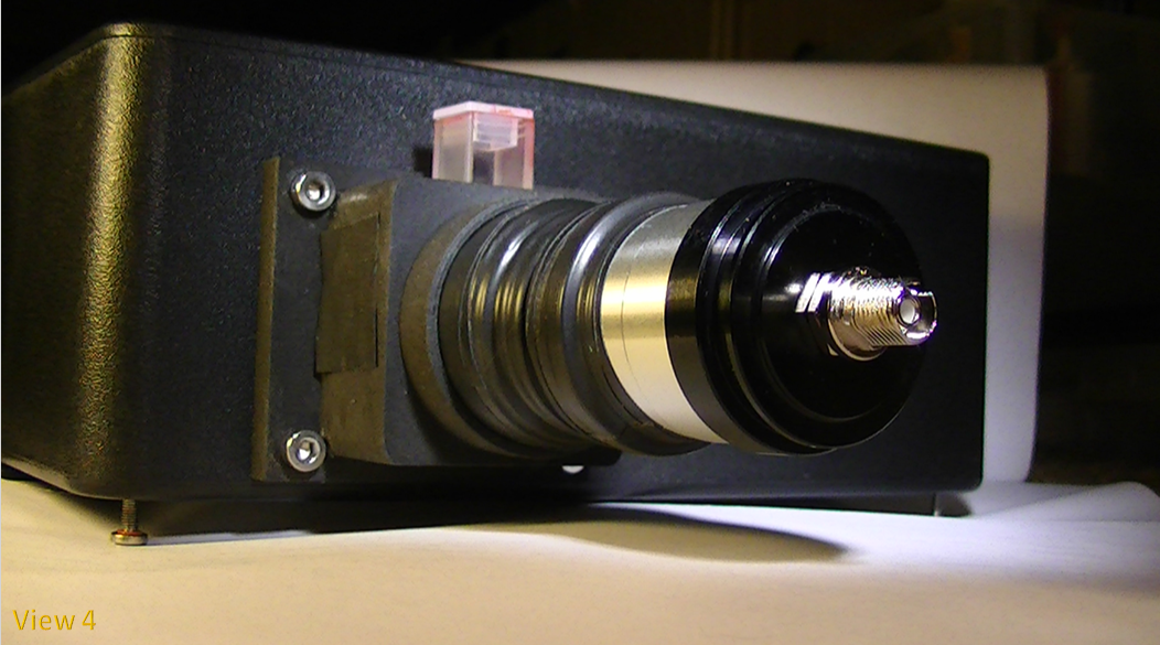
1 Bad A$$ Laser Collimation Tube Assembly! DAV5 V3 Spectrometer Log#40
01/02/2017 at 19:39 • 0 commentsThese pictures and plots are my most recent data results using my redesigned 532nm laser collimation tube assembly;
![]()
![]()
![]()
![]()
![]()
![]()
DAV5 V3.01 Raman Spectrometer
The only thing worth doing, is the thing worth doing right!
 Where
Where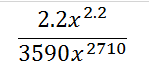


 Focal distance from apex of 32mm lens to mirror is; 70mm. From centerline of mirror to sensor is; 65.02mm.