 ElectroBoy
Soldering is a skill but sometimes we can do it better just by replacing the circuit with Printed Circuit Boards. In this tutorial, we will talk about different PCBs and types of services related with it. Recently, I made a project on LORA (long range radio) using it as a long-range switch. Which then interfaced with Arduino and programmed to send/ receive the strings. For the receiver shield, I used holed prototypes from JLCPCB. JLCPCB is China’s PCB manufacturer deals in services related to printed circuit board and 3D print. It is one stop solution for an electronics hobbyist to work on a hardware project.

Working on professional PCBs is very amazing, just do a little bit of soldering and we are good to go. But sometimes we have to make project fast and we can’t wait for the leading time and shipping time. And for this situation, I made a hole pcb prototype which is same as available in market for making projects except the quality.
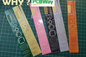
Holed PCB prototypes:

Hole type PCBs are very useful when we have to make a simple project but in a professional way. The spacing of each hole is around 1.254mm which is universal for all the DIP IC packages and through hole components. I generally use 1.2mm thickness which is easy to break the prototype according to the required parameters. That’s why I always prefer to stock some pieces of these boards. Any school and college project can be made on it in a professional way which can be represented in the science fair too.
Holed v/s dedicated PCB:

If you can wait or have more time to build the same project, then Dedicated PCB is recommended over everything. Here you can do a lot of wiring in 6 layers of the same board. It is easy to mount a lot of SMT and TH component in small form factor of the board. These boards are amazing and JLCPCB also offers SMT assembly service starting from just $2. In this the components and assembly process are done by JLCPCB.
Other PCB services:

PCB services also includes full PCBA (Both side DIP and SMT assembly) in standard service, Stencil and 3D printing. JLCPCB may be your next one stop and very reliable solution to all the circuit requirements. See the capabilities offers by JLCPCB from here.
Why JLCPCB and How to order:

Go to JLCPCB > Upload your Gerber files > Choose the material, finishing and color specs > Add the PCB into cart > Checkout and receive your boards in 7 days.
A huge discount on 6 layer PCB:
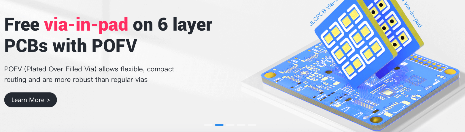
JLCPCB just launched a new offer on 6 layer PCB, get you Quote now for 6 layer ENIG finished PCB for just $20. This offer is only valid till 5 Jan 2023 and this is just an introductory price to new Via-in pad capability.
 Hendra Kusumah
 DIY GUY Chris
 Lithium ION