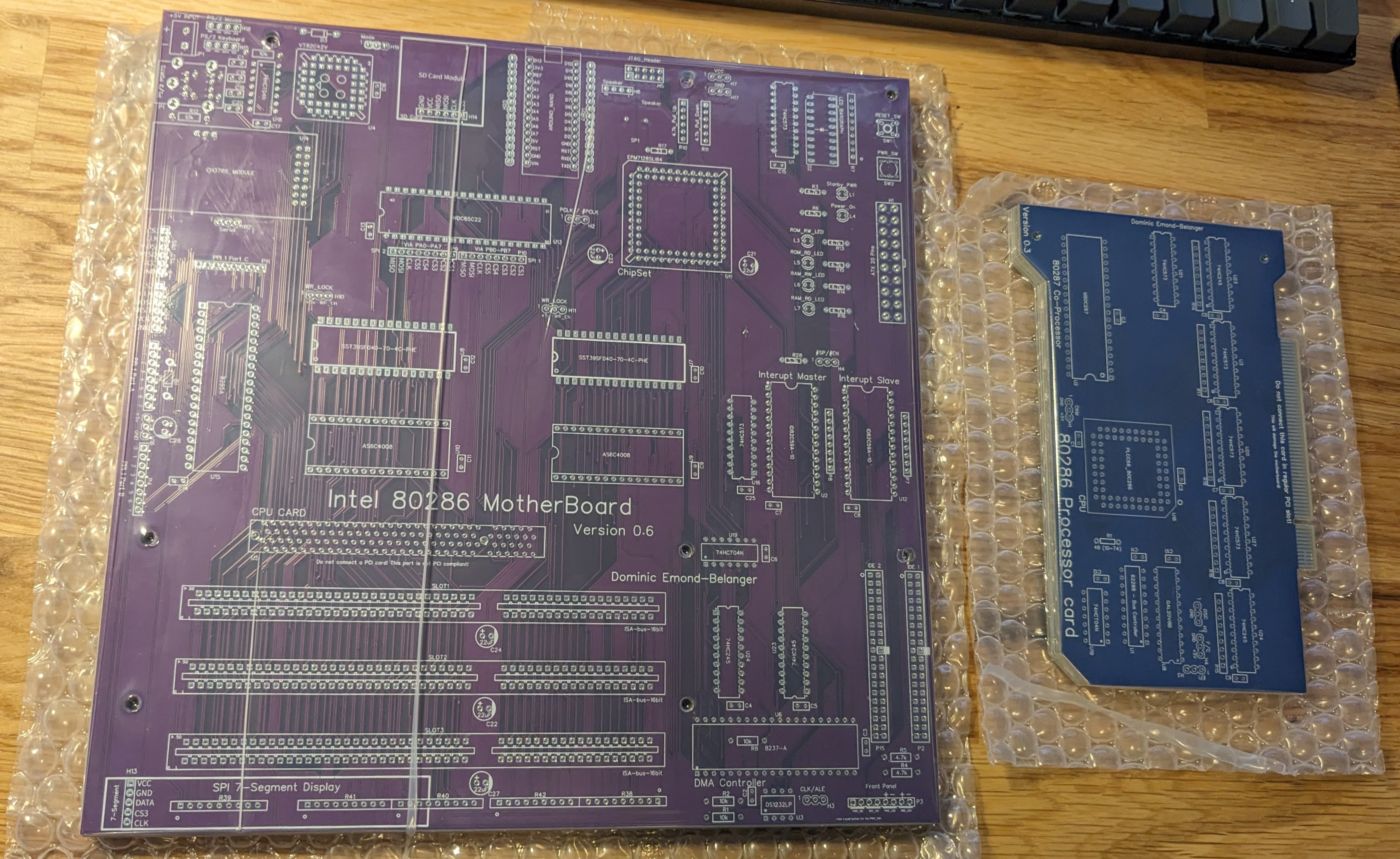
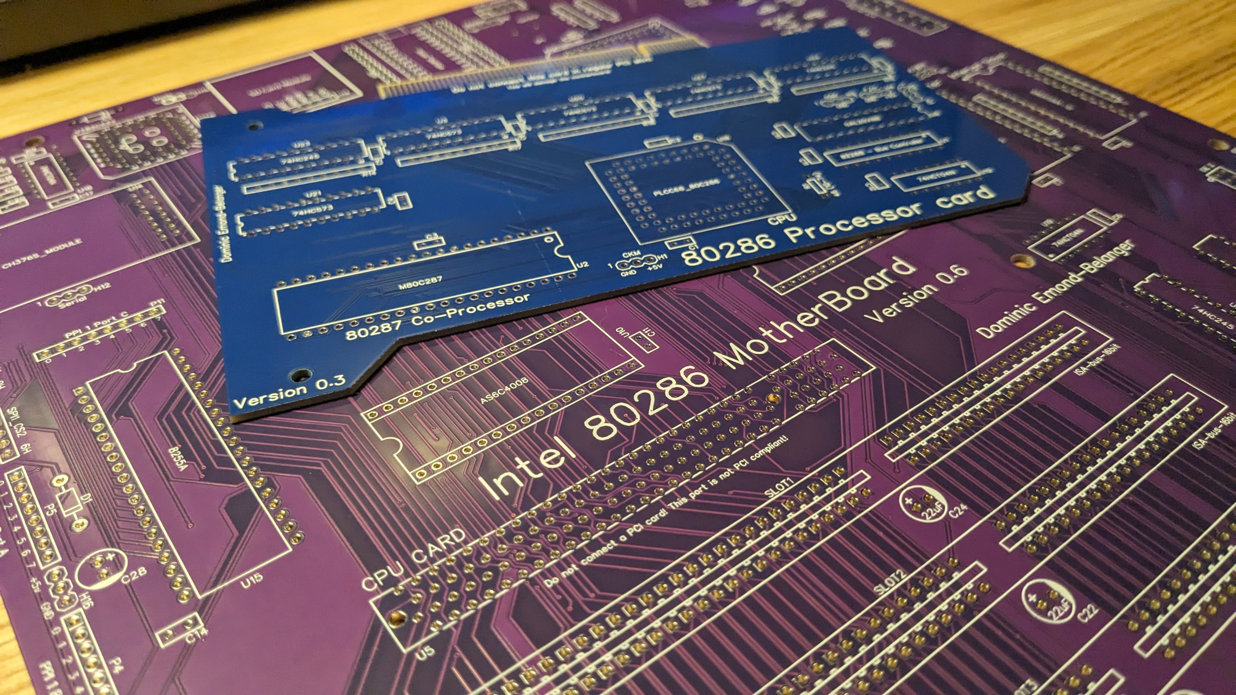
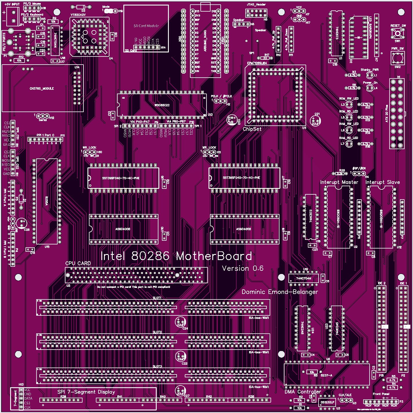
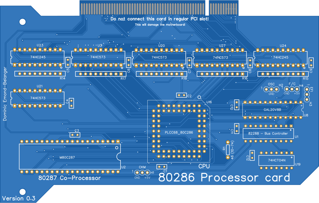
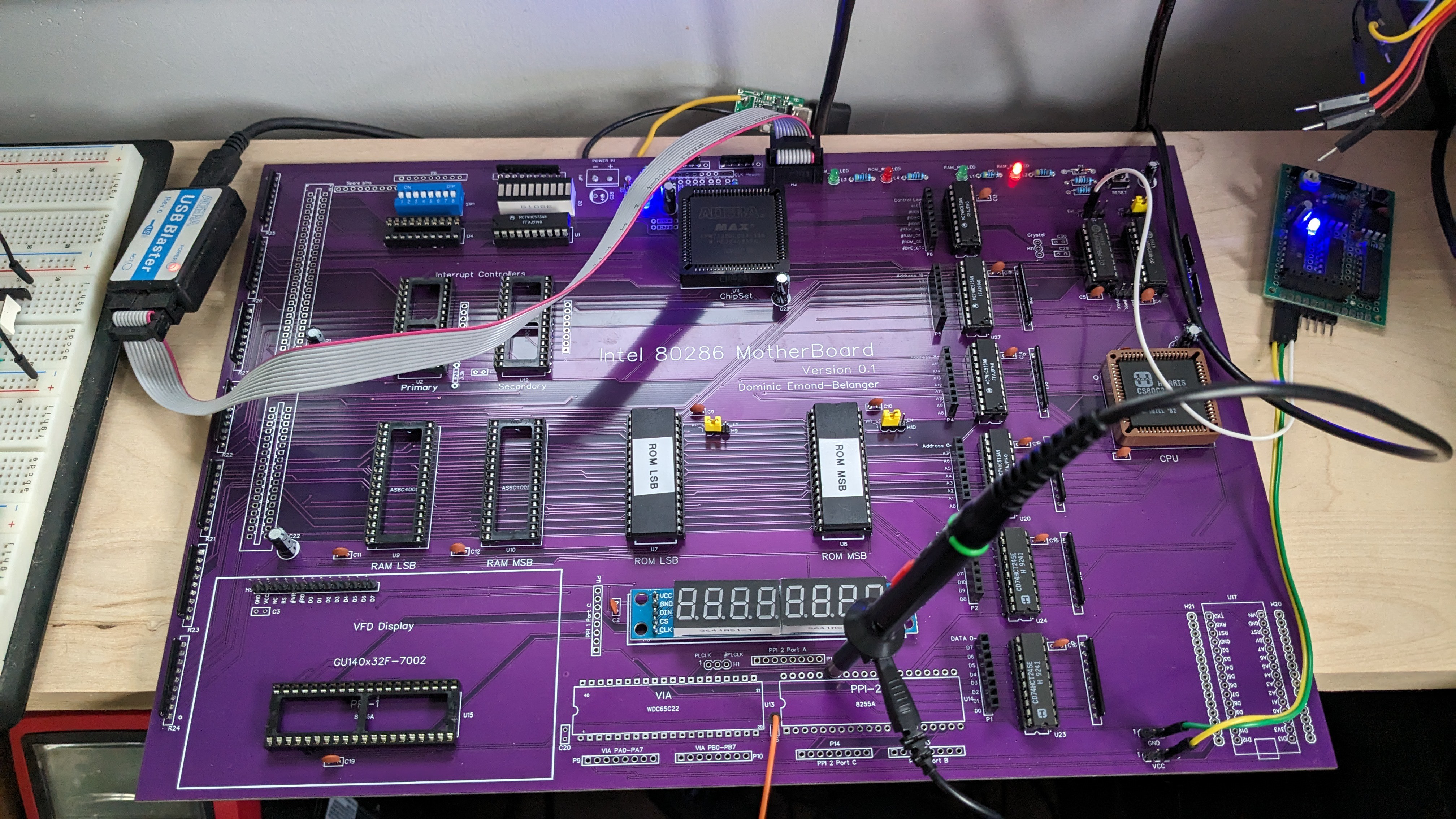
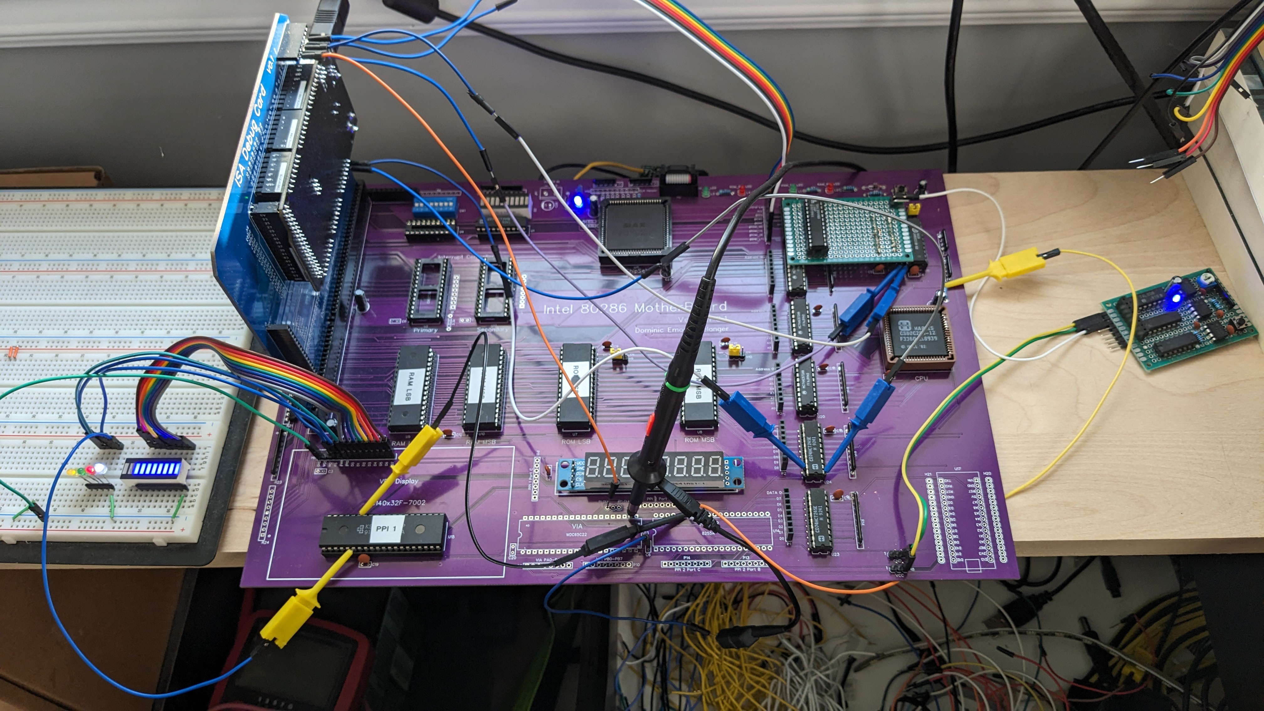
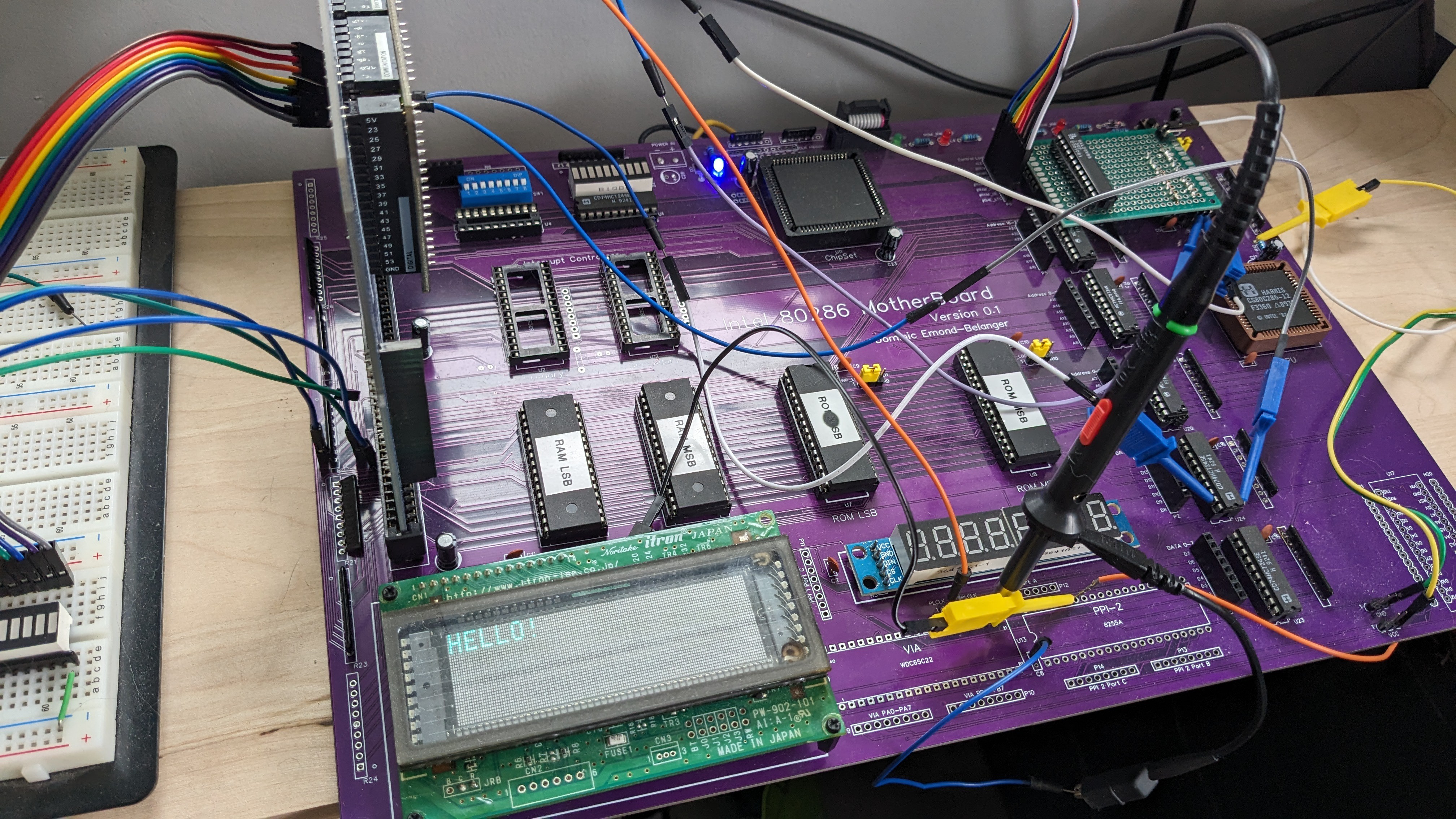
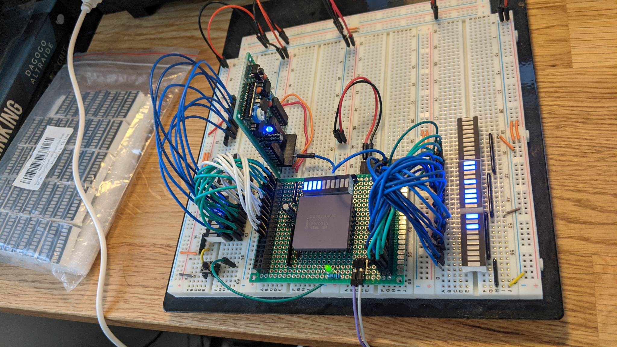
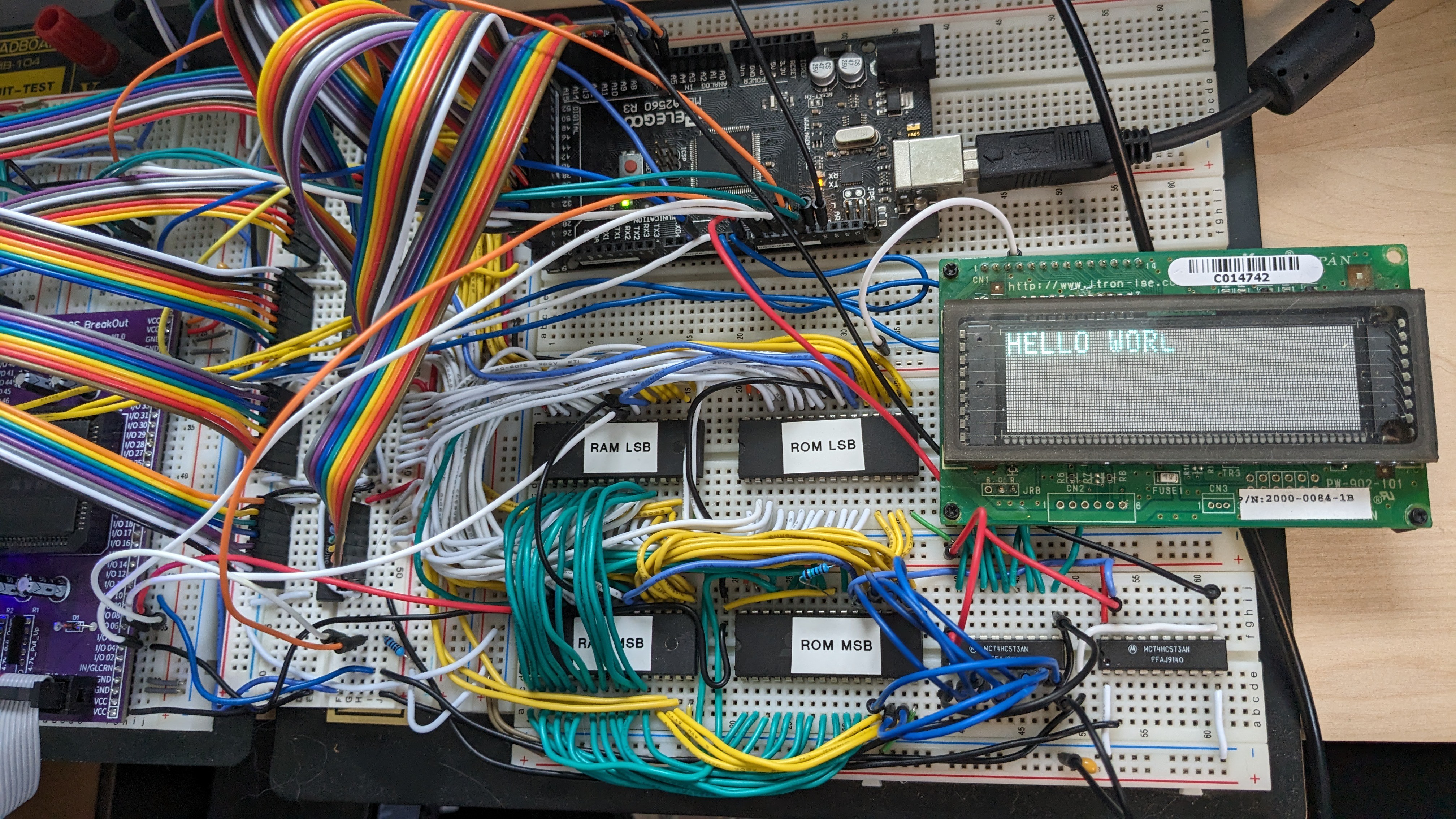
 Dominic Emond-Belanger
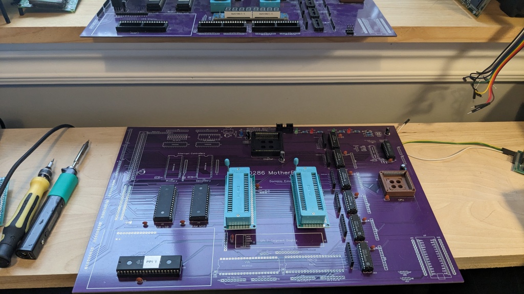
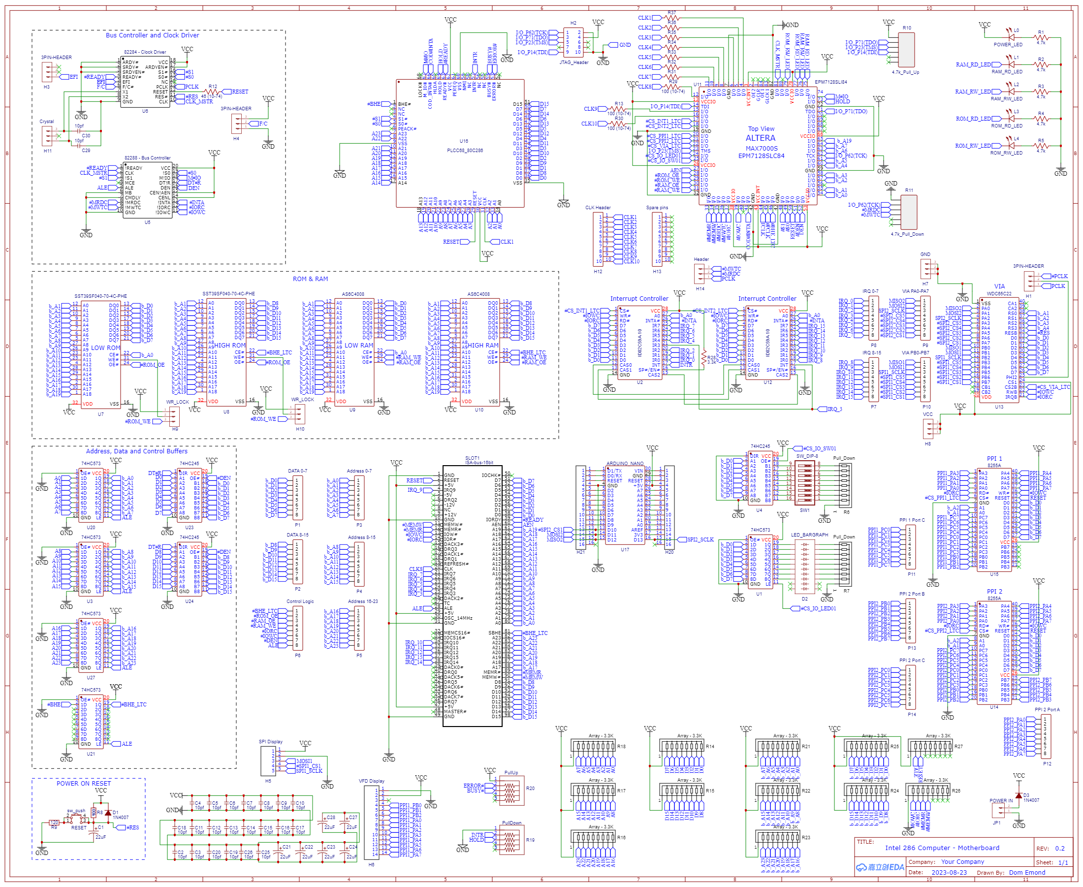
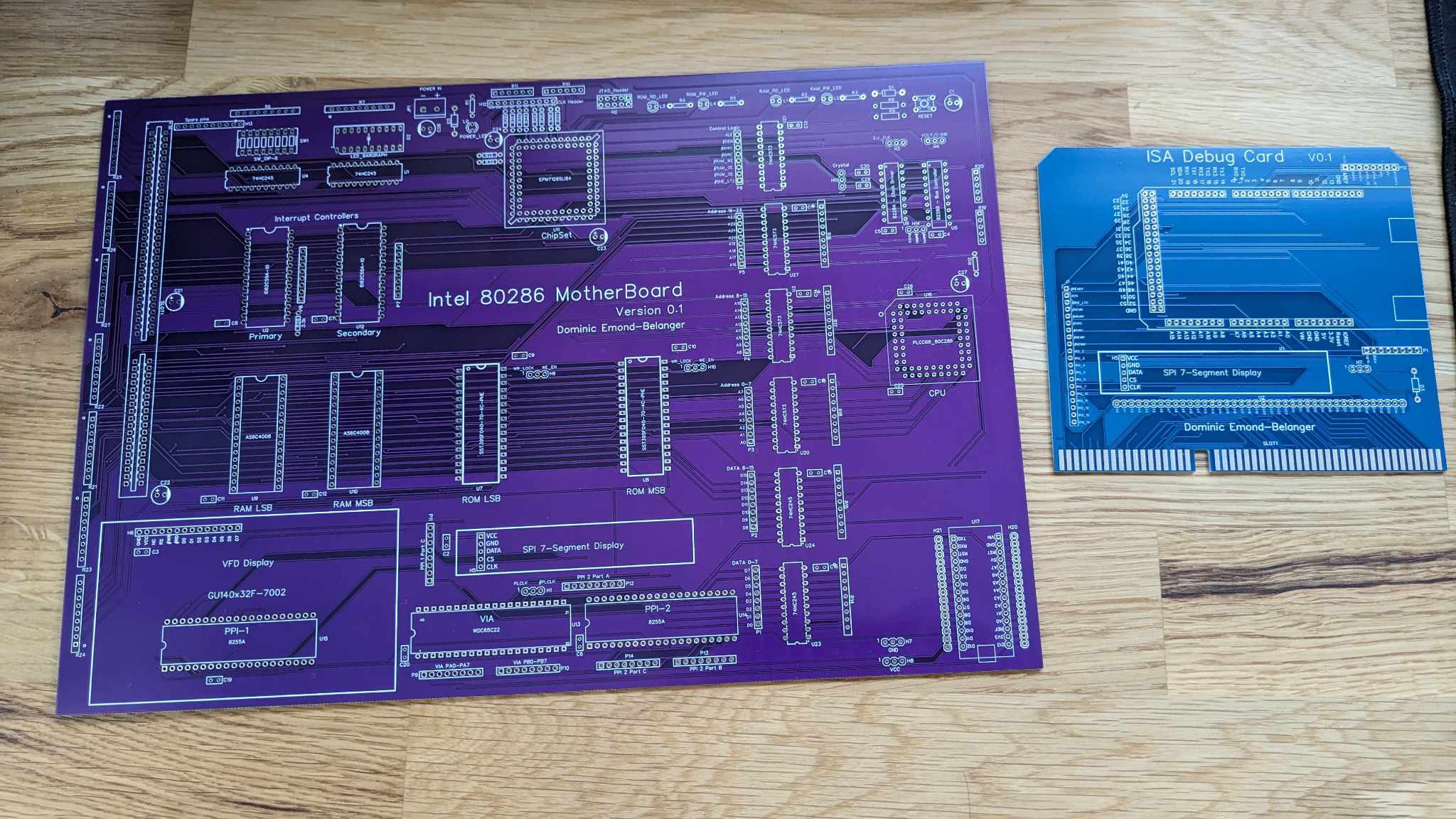
The goal of this project is to learn how to design a AT compatible 286 system and learn x86 assembly.
Current features :
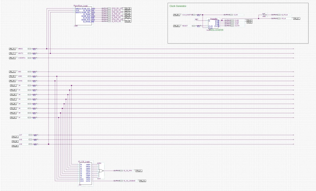
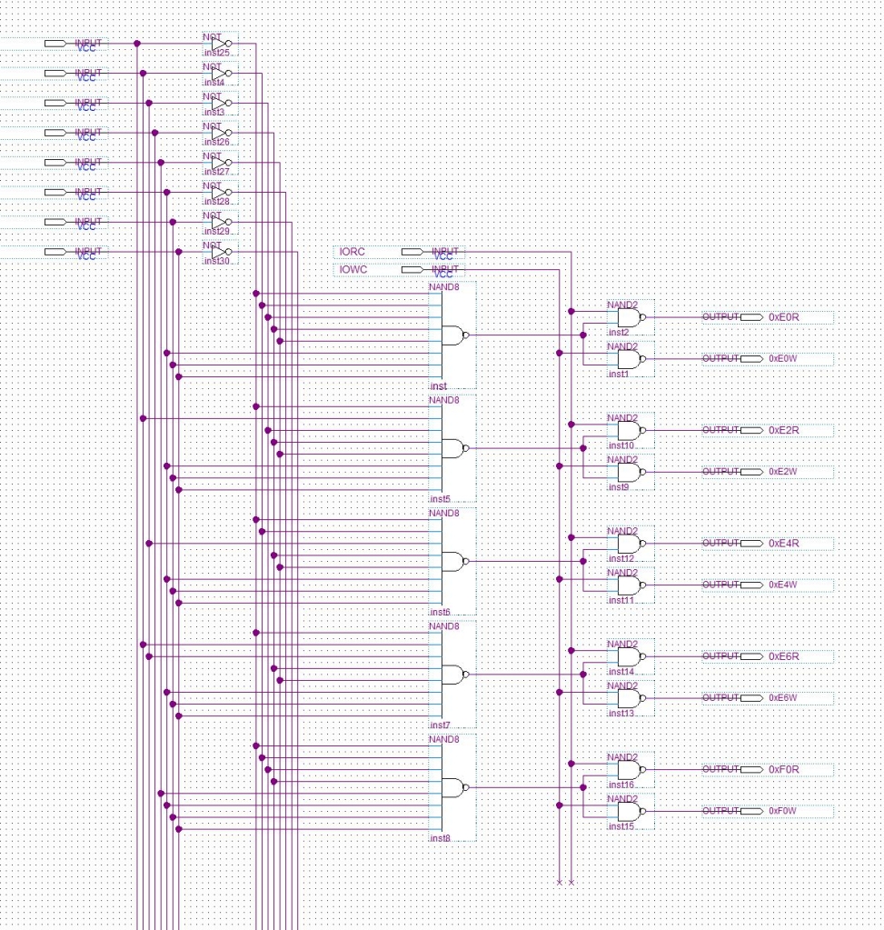
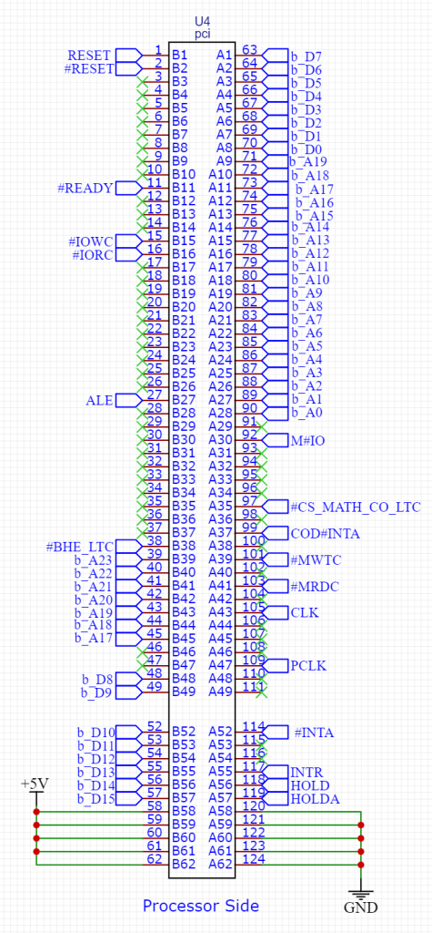
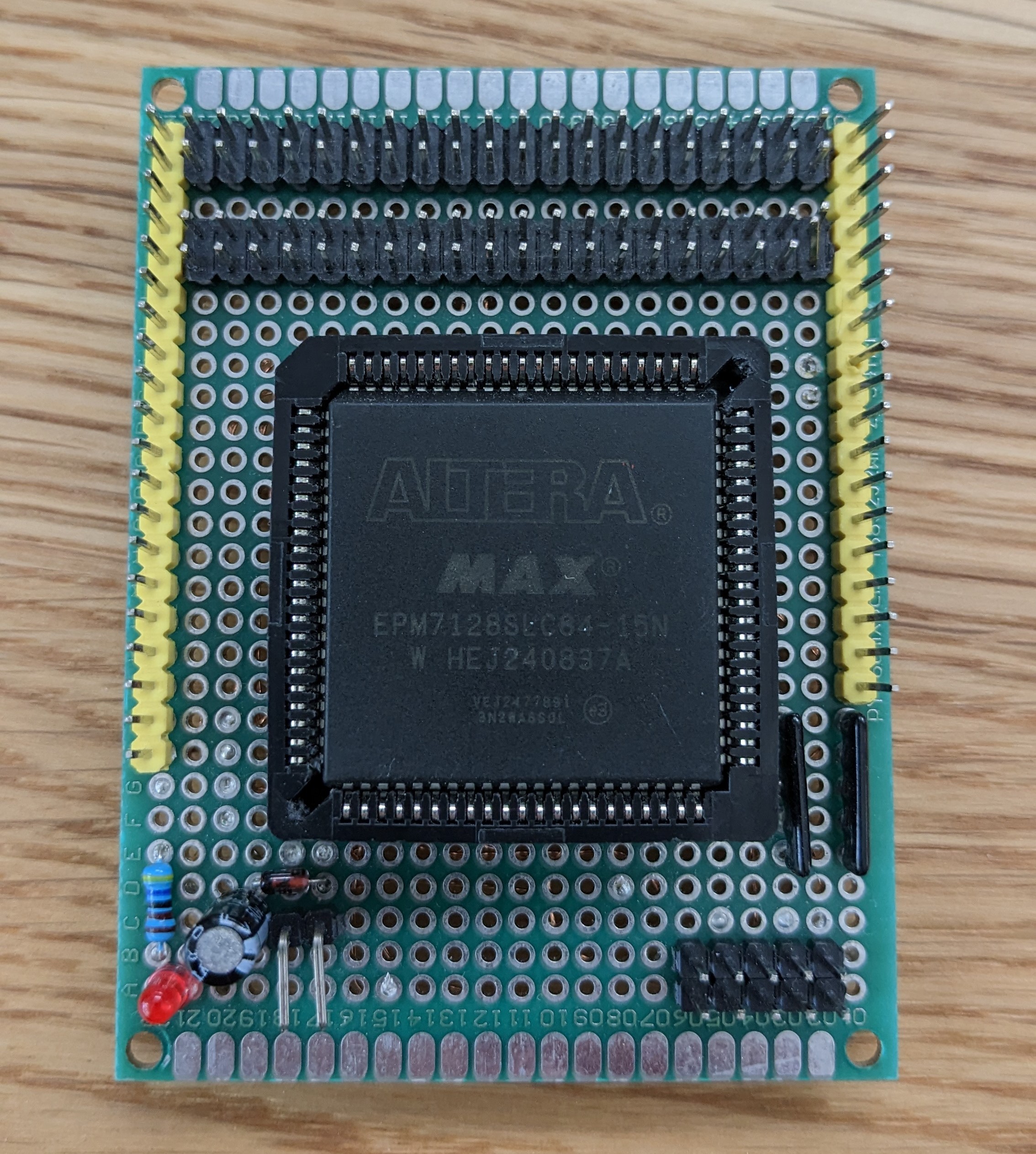
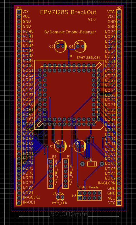
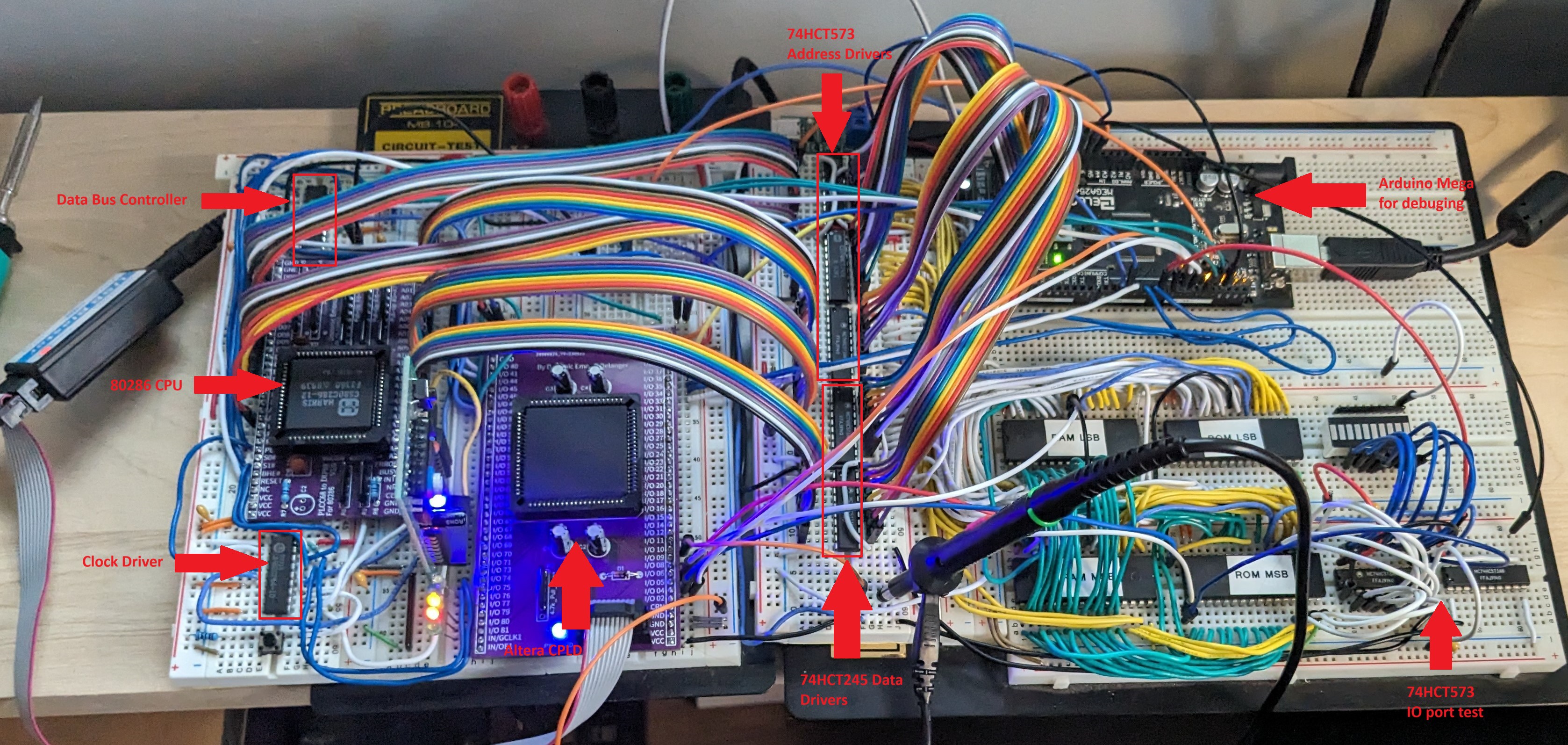
- CPLD "Glue Logic / Chipset"
- ISA 16 bits expansion slot
Features that I would like to have in the near future :
- mATX or ATX motherboard form factor
- PS/2 Keyboard port
- IDE support
- USB flash drive support
Extra features :
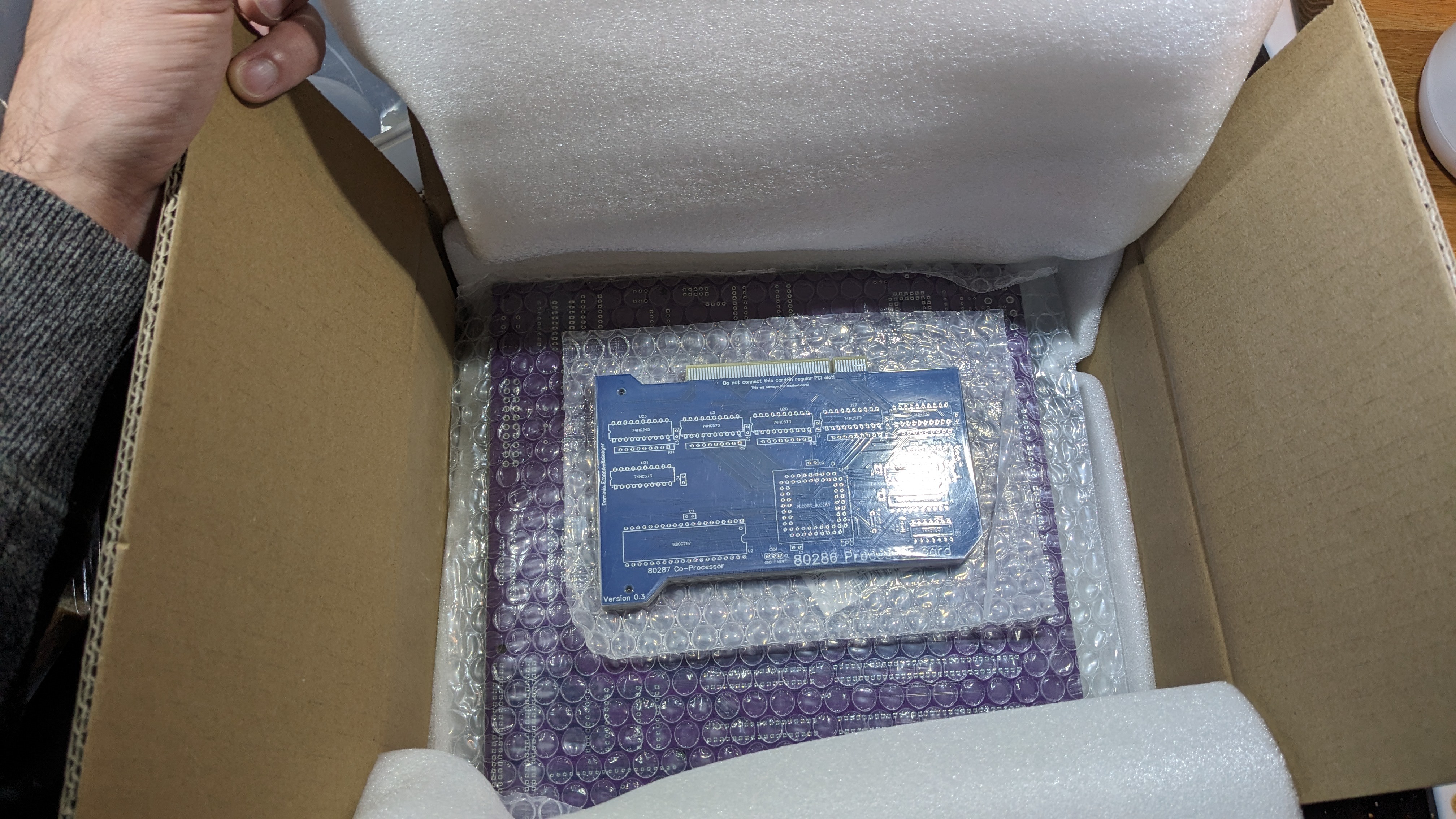
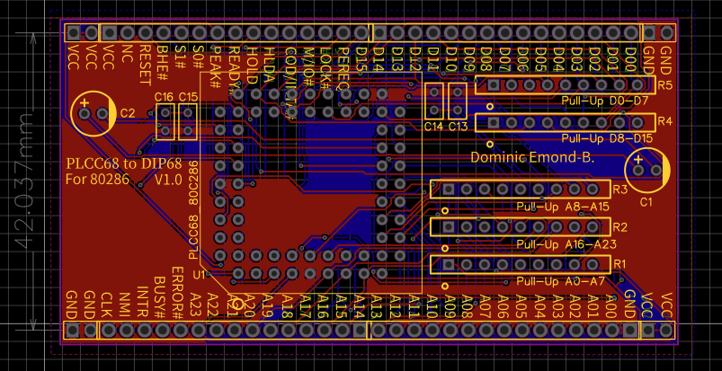
- Modular CPU card (16 bits)
- Custom video card (Onboard or ISA)
- Custom BIOS


 zacnotes
 Jon Buford
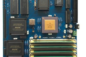
 Tobias Rathje
 Valentin Angelovski
If I were going to design a motherboard for the 286, I would consider using technology from the 1980's. We designed a motherboard by using a chipset. A chipset integrates all the logic on the motherboard into 3 or 4 devices. Consider the NEAT chipset developed by Chips and Technologies for the Intel 80286. A chipset and 286 go together only one way which is described in their datasheets. If you put them together that way the motherboard is guaranteed to work. This turns the motherboard design into a PCB layout project.