 Dave Collins
Scope of the project:
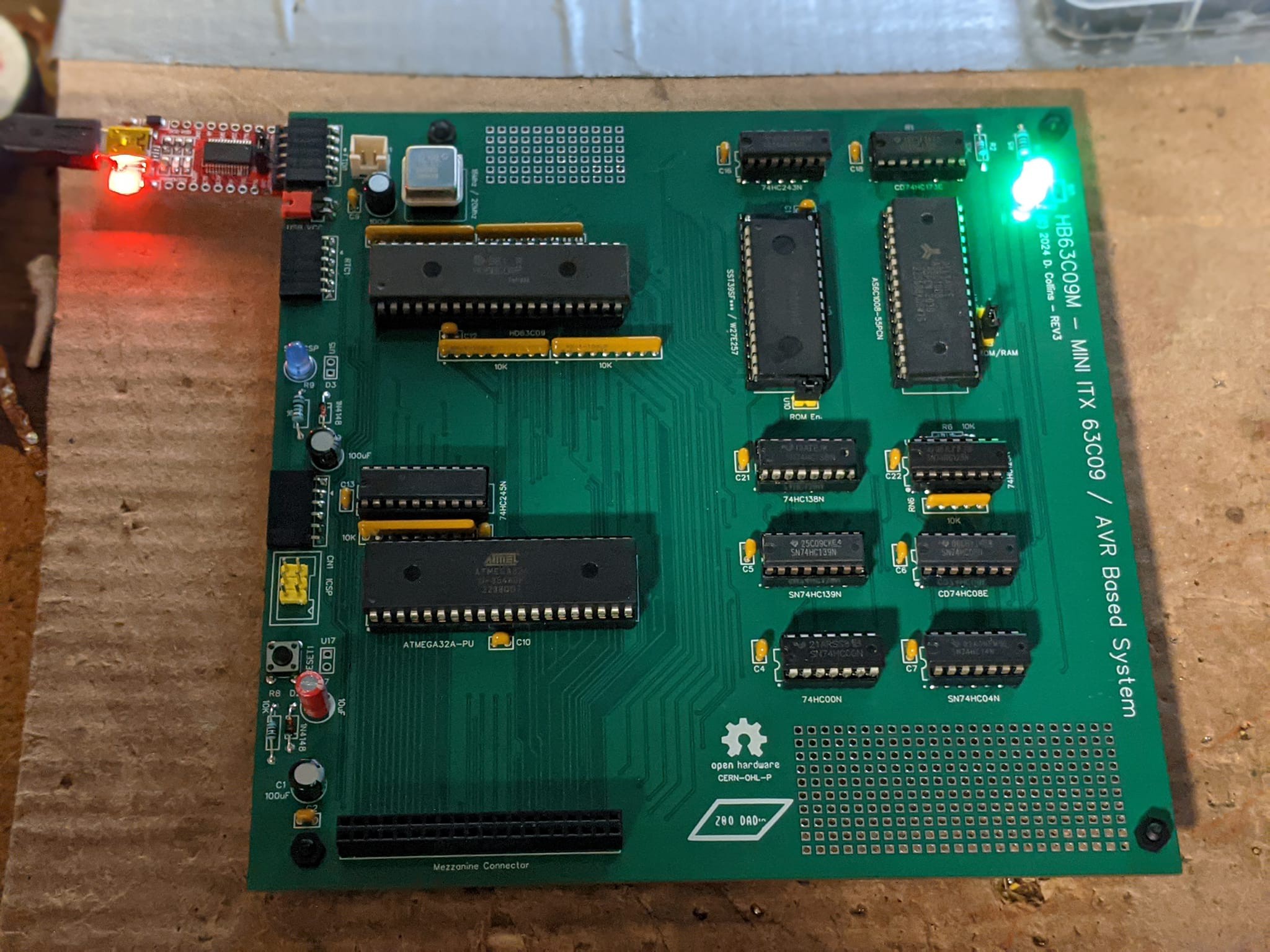
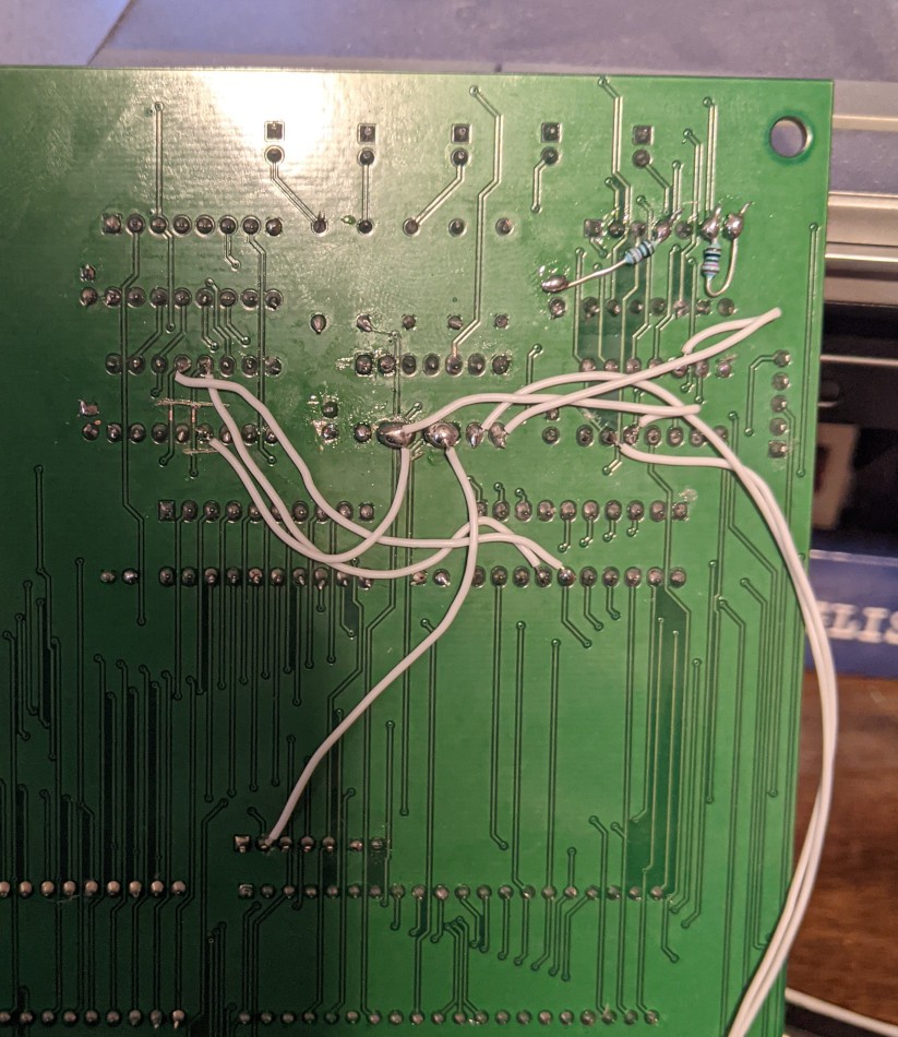
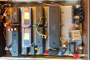
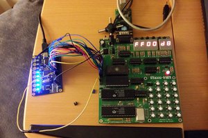
Scope of project is to get a AVR and a 63C09 to share the bus so the 63C09 has access to modern serial protocols, timers and other modern nice stuff. The Current prototype in breadboard form accomplishes this. The PCB prototype will be for finishing the firmware and testing chip set improvements so that we can reduce the chip count.
The running schematics will always be in the files section, thanks for checking out the project
Quick Jumps:
Relevant articles (newest first):
- Sharing the bus with an Arduino without a latch (1/20/24)
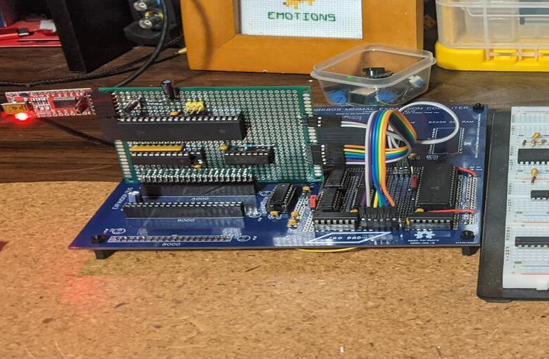
- Hack-a-day Pages: HB63C09 Mezzanine Connection (1/20/24)
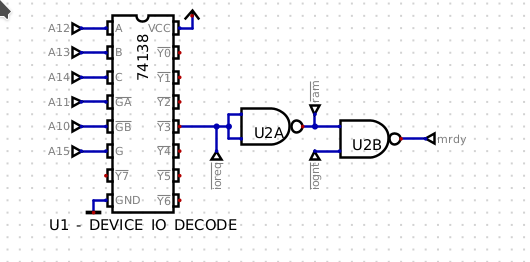
- REV3 Chip set overview ( 1/4/24)
- Hack-a-day Pages: Not all inverters are the same (10/27/23)
- Clock circuit for REV2 based on this article
REV1 PCB Pitfalls (10/21/2023)
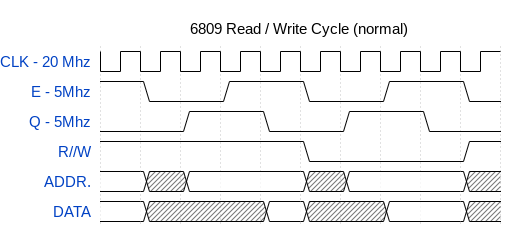
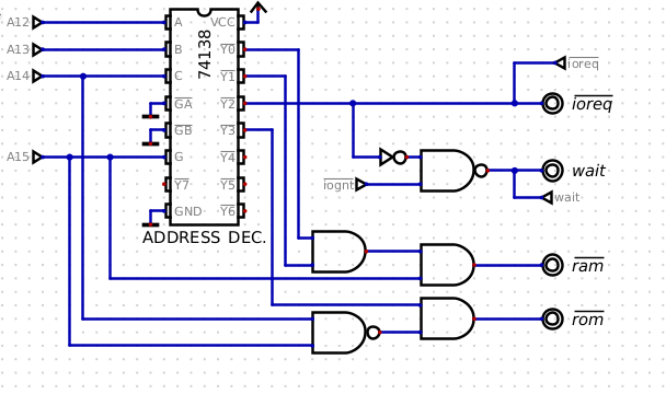
REV1 Architecture overview (10/9/2023)
Files section and license :
AUTODIDACT WARNING!!
I am a HFC designer with the equivalent work experience enough to call myself a civil / mechanical engineer in my day job. Essentially, I design large scale metropolitan area fiber optic and RF utility networks. I have an Associates in Computer Hardware, and an embarrassingly high number of industry certifications from an ongoing 20 year carrier in telecommunications engineering. I don't have any formal EE training but I read A LOT.
I am a hobbyist with over 40 years of practice in the area of home brew computing!
There are aspects of this design which do not, due to a lack of training on my part adhere to what might be commonly held best practices. In general all of my projects should not be considered to adhere to any 'high speed' design principles. I try to verify everything I do on my bench, but everything is 100% at your own risk. I don't make any guarantees, which is outlined in the very easy to understand CERN-OHL-P License
Sponsorship:

Once again, PCB Way has again kindly offered to sponsor the prototyping costs for this project. PCBWay manufactures quality PCB's, 3d prints, as well as does metal fabrication. Additionally they sponsor student projects, and hobbyist's open hardware projects. Talking with any one of their sales staff for even a short amount of time it is clear they truly do care about the next generation of engineers and about the importance of open hardware designs.
Without the generous help offered, it would be difficult for me to complete these projects just simply due to the cost associated, and for that I am truly grateful. So for your next project why not check out the services that they offer?
Thank you, PCBWay


 Tom
Tom
 Jac Goudsmit