 Johnny
FOR SOME REASON I DON'T GET NOTIFIED ABOUT COMMENTS YOU LEAVE, SORRY IF IT TAKES A WHILE FOR ME TO RESPOND.
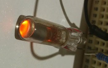
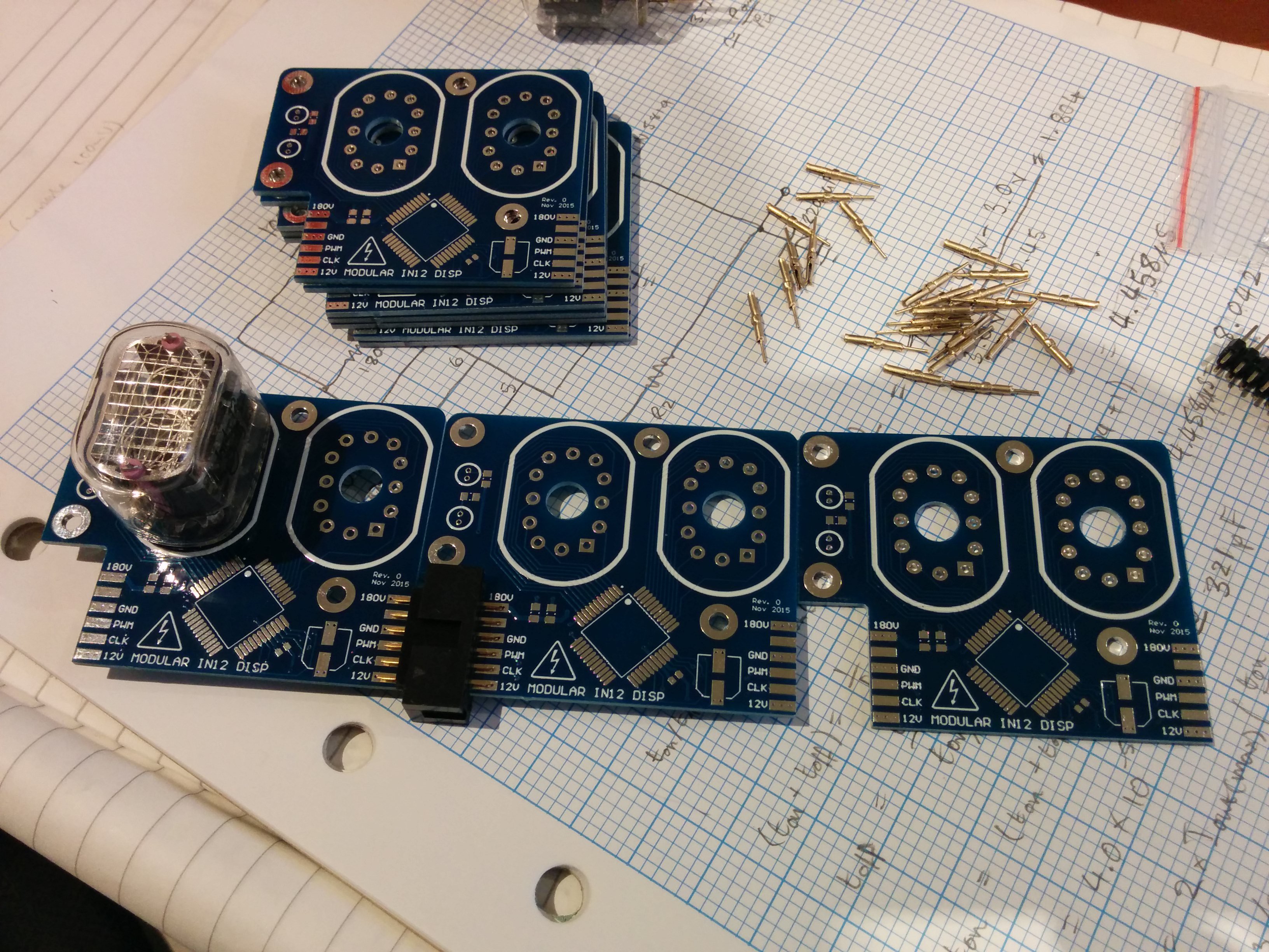
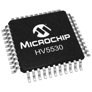
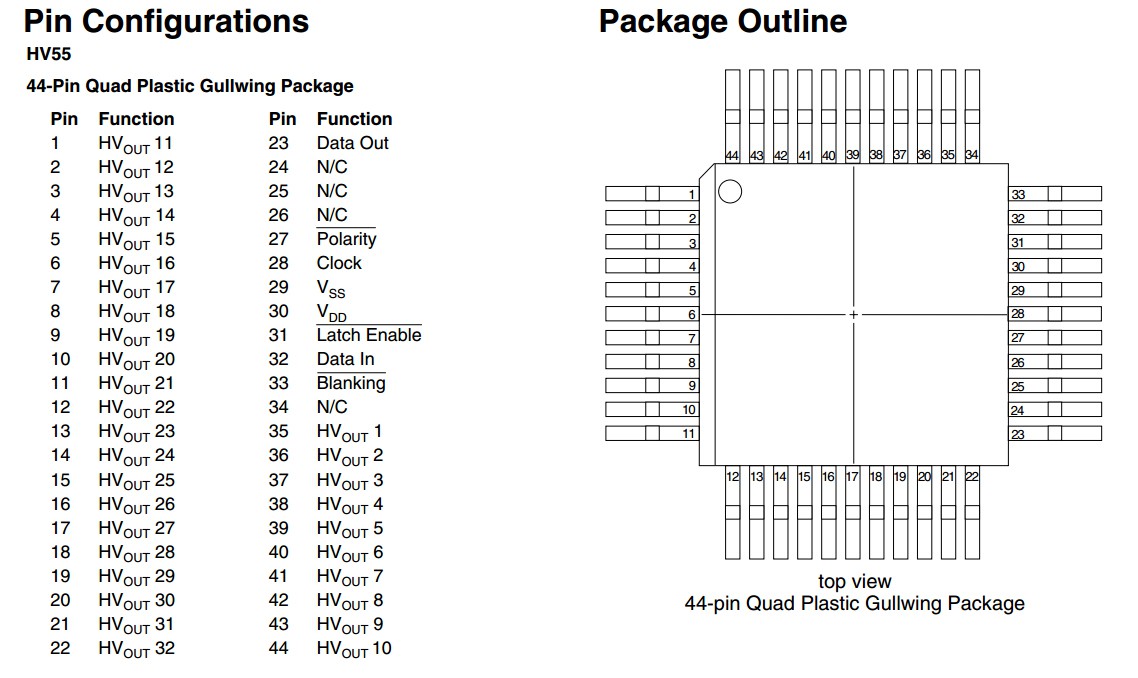
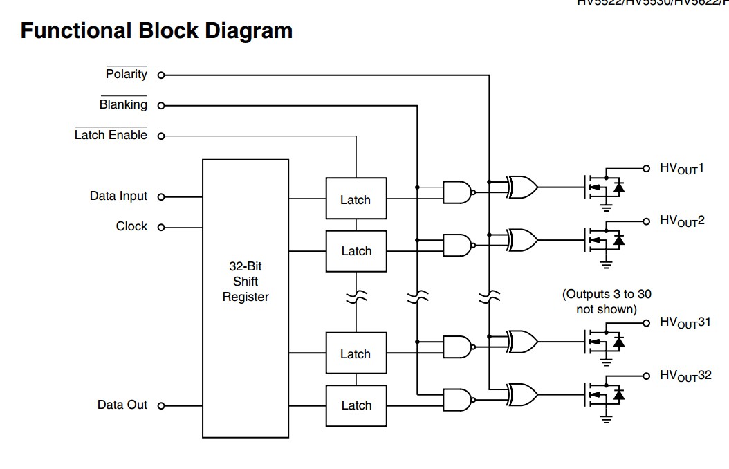
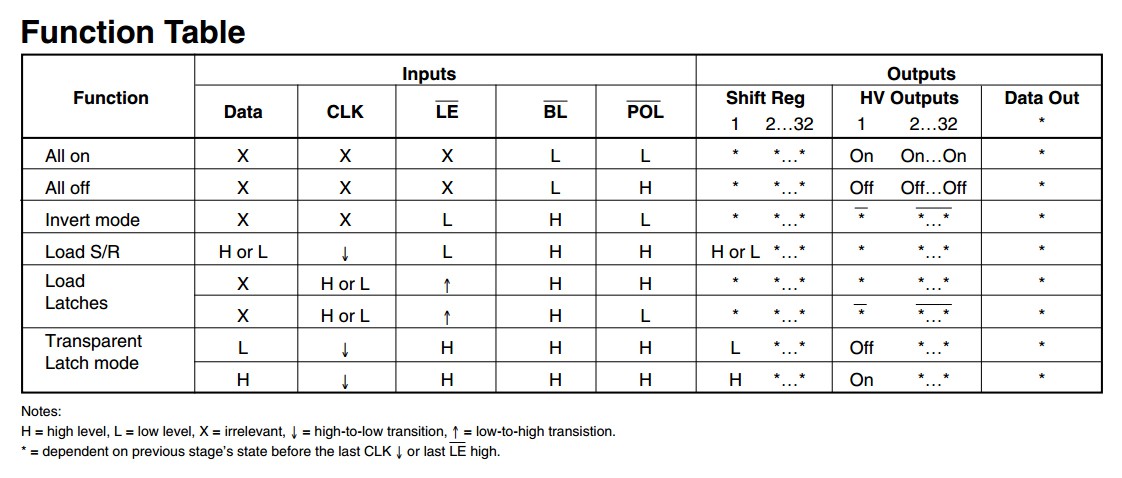
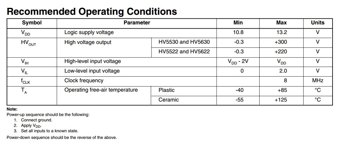
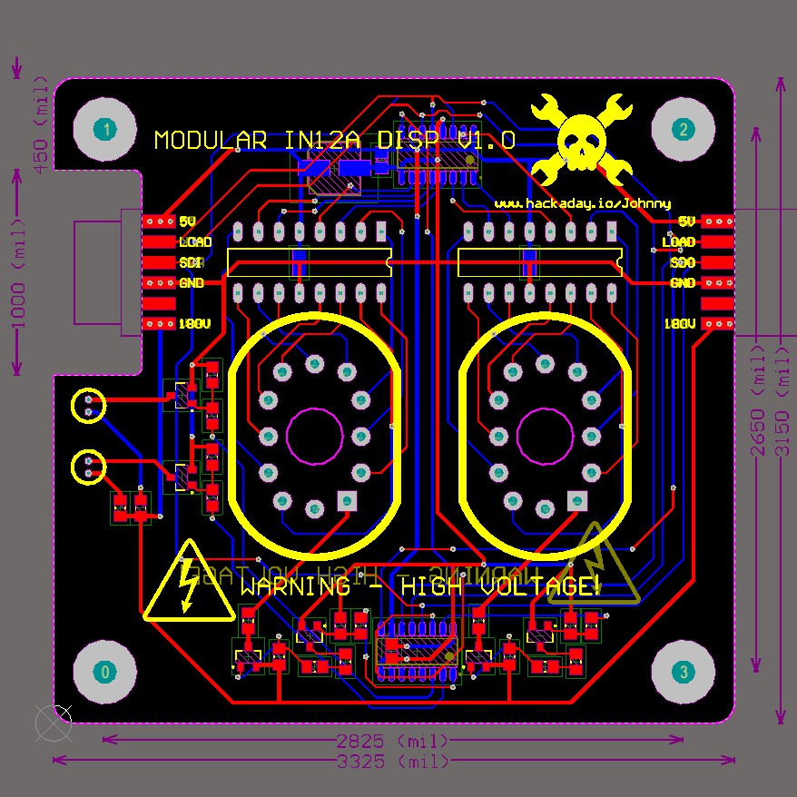
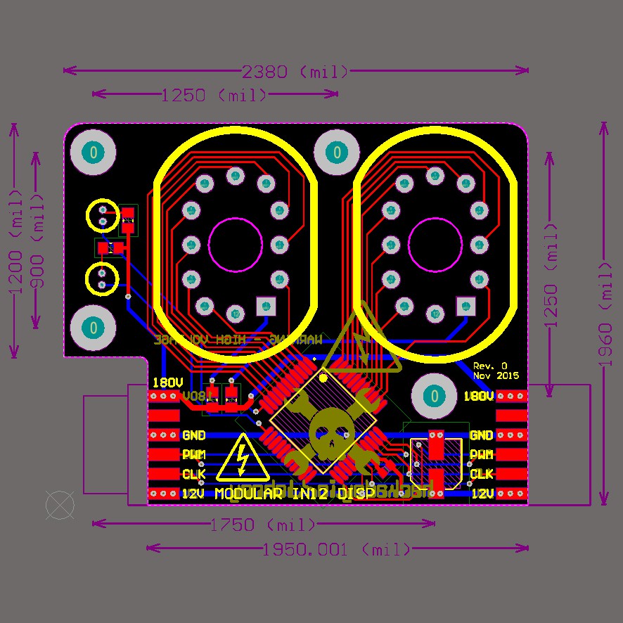
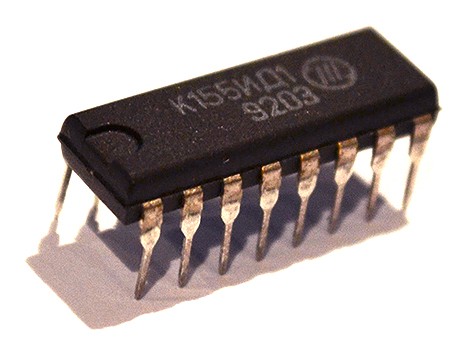
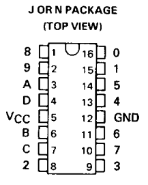
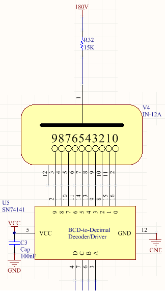
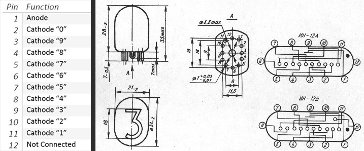
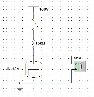
The main objective for this project is to design a modular nixie display board containing two IN12A's and two neon indicators (colon) that can be strung along to create 2, 4 or 6 digit clocks. The idea is, tubes can be individually controlled via SPI. I explored different methods of driving nixies, such as using the common SN74141 BCD to Decimal decoder driver clones called the K155ID1 along with 74HC595 8-bit shift registers. Also shift-registers with high-voltage transistors on the outputs. These methods were ok, but I later changed my design to include the HV5530 instead. The HV5530 is a shift register with high-voltage open-drain outputs and are still being manufactured.


 Marcin Saj
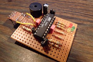
 Klaus Dormann
 John Lonergan
 Electroniclovers123
and there is a firmware to make a watch out of them, and not to test lamps?