Introduction
In a drawer, I had an MC68EC020 lying around; it was ordered along with some 68K parts because it cost less than five bucks. Wouldn't it be wonderful to have your own 68020 system (like the good old Sun-3 system)? But a system that is completely transparent and easy to understand?
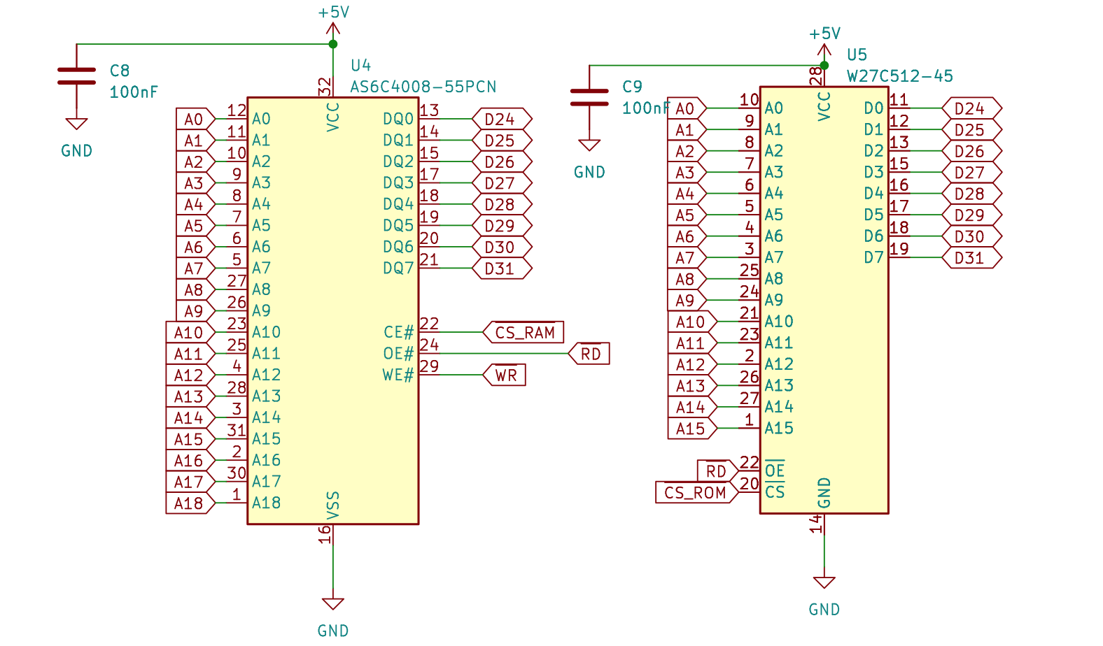
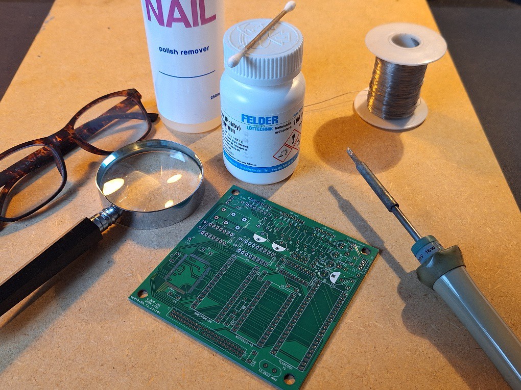
I designed and built a simple single-board computer with this chip, using only conventional ICs - no GAL/PAL or CPLD. It includes just the CPU, EEPROM, RAM, IO and some glue logic.
Specifications
- MC68EC020-FG25 (normal operation 8 to 25 MHz).
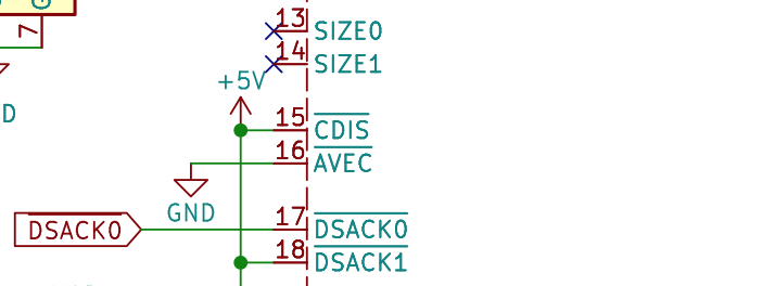
- Selectable zero, one or two wait states.
- 8 bits fixed bus size.
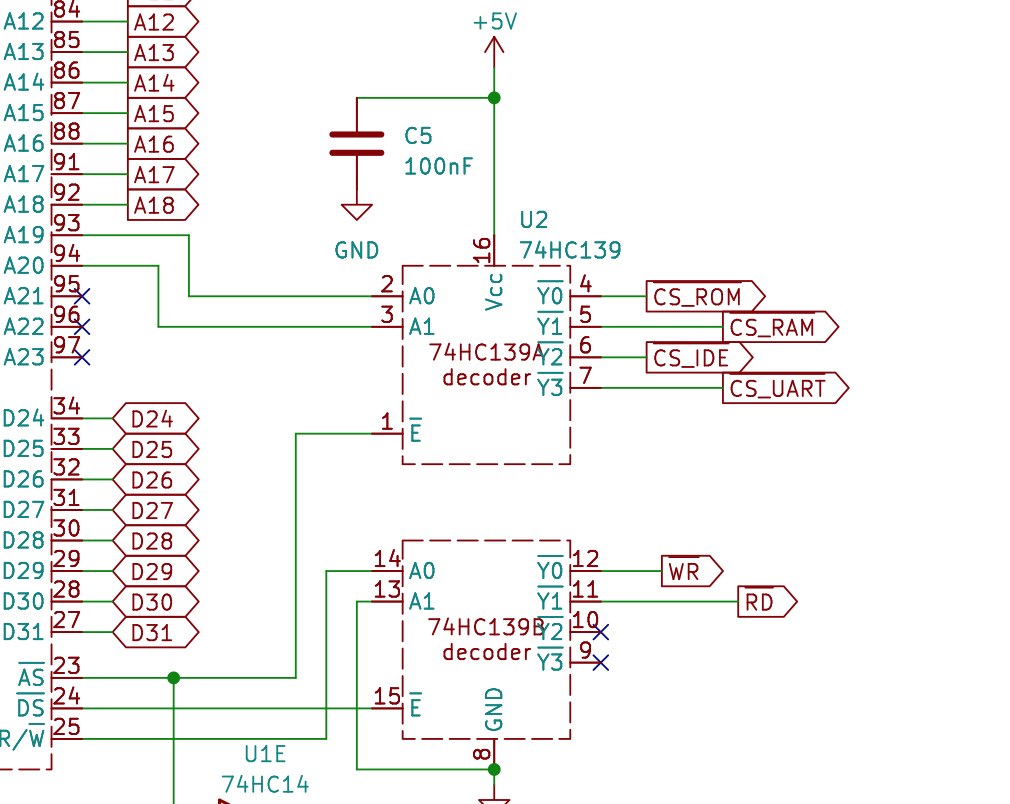
- 512 KB RAM (AS6C4008-55.)
- 64 KB EEPROM (W27C512-45.)
- 16550 UART (addressable only in supervisor mode).
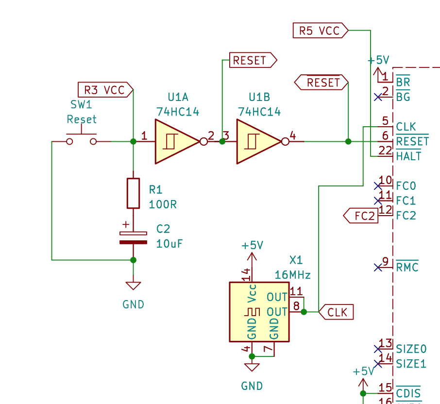
- 100 Hz RC-oscillator (for task switching and simple timings).
- Low power: 200 mA @25Mhz (=1 Watt).
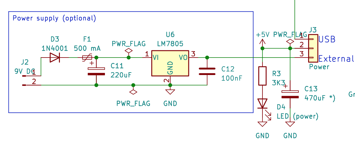
- Optional on board power supply (7805).
- PCB size: only 10 x 10 cm.
Peripherals
- Software I2C for RTC xxx (untested yet).
- Software SPI for SD-card (untested yet).
- IDE/SD-card connector (untested yet).

 Keith
Keith
 Benchoff
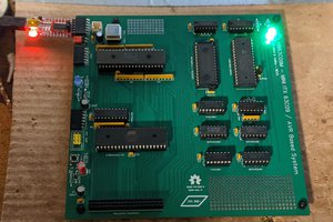
 Dave Collins
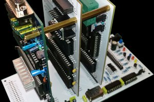
 padnest
Is a PCB board gerber file available or source? The Instrucions say Order the PCB board, but the is no source or gerber file.
Thanks